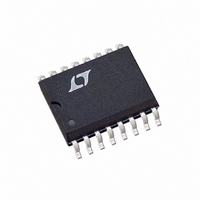
LT1054CSW Linear Technology, LT1054CSW Datasheet

LT1054CSW
Specifications of LT1054CSW
Available stocks
Related parts for LT1054CSW
LT1054CSW Summary of contents
Page 1
... Negative Voltage Doubler ■ Positive Voltage Doubler ■ L, LT, LTC, LTM, Burst Mode, Linear Technology and the Linear logo are registered trademarks and ThinSOT is a trademark of Linear Technology Corporation. All other trademarks are the property of their respective owners. BLOCK DIAGRAM V ...
Page 2
... PART MARKING PACKAGE DESCRIPTION LT1054CN8 8-Lead Plastic DIP LT1054IN8 8-Lead Plastic DIP LT1054MJ8 8-Lead Ceramic DIP 1054 8-Lead Plastic SO 1054L 8-Lead Plastic SO 1054I 8-Lead Plastic SO LT1054CSW 16-Lead Plastic SO LT1054ISW 16-Lead Plastic SO LT1054CJ8 8-Lead Ceramic DIP http://www.linear.com/leadfree/ http://www.linear.com/tapeandreel/ TOP VIEW ...
Page 3
ELECTRICAL CHARACTERISTICS temperature range, otherwise specifications are at T PARAMETER Supply Current Supply Voltage Range Voltage Loss (V – OUT Output Resistance Oscillator Frequency Reference Voltage Regulated Voltage Line Regulation Load Regulation Maximum Switch Current Supply Current ...
Page 4
LT1054/LT1054L TYPICAL PERFORMANCE CHARACTERISTICS Shutdown Threshold 0.6 0.5 V PIN1 0.4 0.3 0.2 0.1 0 – 50 – 100 TEMPERATURE (°C) LT1054 • TPC01 Supply Current in Shutdown 120 100 PIN1 80 ...
Page 5
TYPICAL PERFORMANCE CHARACTERISTICS Regulated Output Voltage –4.7 –4.8 –4.9 –5.0 –5.1 –11.6 –11.8 –12.0 –12.2 –12.4 –12.6 – –25 TEMPERATURE (°C) PIN FUNCTIONS FB/SHDN (Pin 1): Feedback/Shutdown Pin. This pin has two functions. Pulling Pin 1 below the ...
Page 6
LT1054/LT1054L PIN FUNCTIONS transistor must be added as shown in Figure 1. This will prevent V (Pin 5) from being pulled above the ground OUT pin (Pin 3) during start-up. Any small, general purpose transistor such as 2N2222 or 2N2219 ...
Page 7
PIN FUNCTIONS is charging, the peak supply current will be approximately equal to 2.2 times the output current. During the time that C is delivering charge to C the supply current drops IN OUT to approximately 0.2 times the output ...
Page 8
LT1054/LT1054L APPLICATIONS INFORMATION R3 FB/SHDN CAP + 10µF GND TANTALUM CAP RESTART SHUTDOWN ) ) ) ) | | | | OUT OUT = + 1 ≈ 1.21V REF – ...
Page 9
APPLICATIONS INFORMATION where dV = peak-to-peak ripple and f = oscillator frequency. For output capacitors with significant ESR a second term must be added to account for the voltage step at the switch transitions. This step is approximately equal to: ...
Page 10
LT1054/LT1054L TYPICAL APPLICATIONS Basic Voltage Inverter + FB/SHDN V + CAP OSC + LT1054 100µF GND V REF – CAP V OUT Negative Voltage Doubler + FB/SHDN V + CAP OSC + LT1054 V GND V IN REF 100µF – ...
Page 11
TYPICAL APPLICATIONS +V OUT OUT –V OUT 5µF FB/SHDN + CAP OSC + LT1054 #1 10µF GND V REF – CAP V OUT 10k INPUT TTL 10k OR CMOS LOW FOR ON 0.022µF 1 ...
Page 12
LT1054/LT1054L TYPICAL APPLICATIONS V IN 3.5V TO 5.5V 20k 1N914 1N914 1N914 + 10µ 3. OUT I = 50mA OUT(MAX) FB/SHDN + CAP LT1054 #1 10 GND 10µF 1/2W – CAP + ...
Page 13
PACKAGE DESCRIPTION CORNER LEADS OPTION .045 – .068 (1.143 – 1.650) FULL LEAD OPTION .300 BSC (7.62 BSC) .008 – .018 (0.203 – 0.457) NOTE: LEAD DIMENSIONS APPLY TO SOLDER DIP/PLATE OR TIN PLATE LEADS .400* (10.160) MAX 8 7 ...
Page 14
LT1054/LT1054L PACKAGE DESCRIPTION .245 MIN .030 ±.005 TYP RECOMMENDED SOLDER PAD LAYOUT .010 – .020 (0.254 – 0.508) .008 – .010 (0.203 – 0.254) NOTE: 1. DIMENSIONS IN 2. DRAWING NOT TO SCALE 3. THESE DIMENSIONS DO NOT INCLUDE MOLD ...
Page 15
... The LTC1054MJ8 is now available. Changes reflected throughout the data sheet Information furnished by Linear Technology Corporation is believed to be accurate and reliable. However, no responsibility is assumed for its use. Linear Technology Corporation makes no representa- tion that the interconnection of its circuits as described herein will not infringe on existing patent rights. ...
Page 16
... V : 1.2V, 1.5V 35µA, ThinSOT IN OUT Q : 2.7V to 5.5V 0.9V to 1.6V, 1.2V, 1.5V OUT : 2.7V to 5.5V 0.9V to 1.6V 50µA, DFN12 IN OUT Q LT 1210 REV F • PRINTED IN USA LINEAR TECHNOLOGY CORPORA TION 2010 0.002µF –V OUT LT1054 • TA14 = 9µA, Q 1054lff ...


