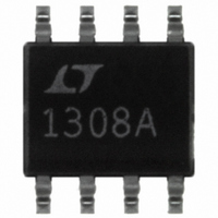
LT1308ACS8 Linear Technology, LT1308ACS8 Datasheet

LT1308ACS8
Specifications of LT1308ACS8
Available stocks
Related parts for LT1308ACS8
LT1308ACS8 Summary of contents
Page 1
... The LT1308A/LT1308B are available in the 8-lead SO and the 14-lead TSSOP packages. L, LT, LTC, LTM, Burst Mode, Linear Technology and the Linear logo are registered trademarks of Linear Technology Corporation. All other trademarks are the property of their respective owners. ...
Page 2
... LT1308AIS8#TRPBF LT1308BCS8#PBF LT1308BCS8#TRPBF LT1308BIS8#PBF LT1308BIS8#TRPBF LT1308ACF#PBF LT1308ACF#TRPBF LT1308BCF#PBF LT1308BCF#TRPBF LEAD BASED FINISH TAPE AND REEL LT1308ACS8 LT1308ACS8#TR LT1308AIS8 LT1308AIS8#TR LT1308BCS8 LT1308BCS8#TR LT1308BIS8 LT1308BIS8#TR LT1308ACF LT1308ACF#TR LT1308BCF LT1308BCF#TR Consult LTC Marketing for parts specifi ed with wider operating temperature ranges. For more information on lead free part marking, go to: This product is only offered in trays ...
Page 3
ELECTRICAL CHARACTERISTICS range, otherwise specifi cations are 25°C. Commercial Grade 0°C to 70° SYMBOL PARAMETER I Quiescent Current Q V Feedback Voltage Pin Bias Current B Reference Line Regulation Minimum Input Voltage ...
Page 4
... Exposure to any Absolute Maximum Rating condition for extended periods may affect device reliability and lifetime. Note 2: The LT1308ACS8, LT1308ACF , LT1308BCS8 and LT1308BCF are designed, characterized and expected to meet the industrial temperature limits, but are not tested at –40°C and 85°C. I grade devices are guaranteed over the – ...
Page 5
TYPICAL PERFORMANCE CHARACTERISTICS LT1308B 12V Output Effi ciency 3. 100 LOAD CURRENT (mA) 1308A/B G04 SHDN Pin Bias Current vs Voltage 50 ...
Page 6
LT1308A/LT1308B PIN FUNCTIONS (SO/TSSOP) V (Pin 1/Pin 1): Compensation Pin for Error Amplifi er. C Connect a series RC from this pin to ground. Typical values are 47kΩ and 100pF. Minimize trace area (Pin 2/Pin 2): Feedback ...
Page 7
BLOCK DIAGRAMS 40k V OUT R1 (EXTERNAL (EXTERNAL) Figure 2a. LT1308A/LT1308B Block Diagram (SO-8 Package 40k 40k V OUT R1 (EXTERNAL ...
Page 8
LT1308A/LT1308B APPLICATIONS INFORMATION OPERATION The LT1308A combines a current mode, fi xed frequency PWM architecture with Burst Mode micropower opera- tion to maintain high effi ciency at light loads. Operation can be best understood by referring to the block diagram ...
Page 9
APPLICATIONS INFORMATION Waveforms for a LT1308B 5V to 12V boost converter using a 10μF ceramic output capacitor are pictured in Figures 4 and 5. In Figure 4, the converter is operating in continuous mode, delivering a load current of approximately ...
Page 10
LT1308A/LT1308B APPLICATIONS INFORMATION LBI LBO GROUND PLANE SHUTDOWN 3 12 LT1308A 4 11 LT1308B 10 5 MULTIPLE VIAs GND V OUT Figure 7. Recommended Component Placement for ...
Page 11
APPLICATIONS INFORMATION SHDN PIN The LT1308A/LT1308B SHDN pin is improved over the LT1308. The pin does not require tying to V the device, but needs only a logic level signal. The voltage on the SHDN pin can vary from 1V ...
Page 12
LT1308A/LT1308B APPLICATIONS INFORMATION V OUT 1V/DIV I L1 2A/DIV V SHDN 5V/DIV 500μs/DIV Figure 14. 5V Boost Converter of Figure 1. Start-Up from 3V Input into 5Ω Load V OUT 2V/DIV I SW 2A/DIV V SHDN 5V/DIV 500μs/DIV Figure 15. ...
Page 13
APPLICATIONS INFORMATION 12V V OUT 5V/DIV 1A/DIV V SHDN 10V/DIV 50μs/DIV Figure 17. Start-Up Waveforms of Figure 16’s Circuit without Soft-Start Components 12V V OUT 1A/DIV V SHDN 10V/DIV 5ms/DIV Figure 18. Start-Up Waveforms ...
Page 14
LT1308A/LT1308B APPLICATIONS INFORMATION Ceramic Capacitors Multilayer ceramic capacitors have become popular, due to their small size, low cost, and near-zero ESR. Ceramic capacitors can be used successfully in LT1308A/LT1308B designs provided loop stability is considered. A tantalum capacitor has some ...
Page 15
APPLICATIONS INFORMATION V OUT 500mV/DIV I L1 1A/DIV 500mA LOAD CURRENT 50mA 200μs/DIV Figure 23. Load Step Response with 10μF X5R Ceramic Output Capacitor and C GSM AND CDMA PHONES The LT1308A/LT1308B are suitable for converting a single Li-Ion cell ...
Page 16
LT1308A/LT1308B TYPICAL APPLICATIONS C1:TAIYO-YUDEN JMK212BJ475MG C2, C3:TAIYO-YUDEN LMK325BJ106MN C4, C5, C6:TAIYO-YUDEN EMK212BJ105MG D1: MBRM120 D2,D3,D4: BAT54S L1: TOKO 817FY-4R7M AV 500mV/DIV 500mV/DIV 500mV/DIV 800mA I LOAD 200mA 16 Triple Output TFTLCD Bias Supply D2 C4 1μF 0.22μF ...
Page 17
TYPICAL APPLICATIONS 3.3V REGULATED Q1 C1: AVX TAJC476M010 C2: VITRAMON VJ225Y105KXCAT D1: BAT54 D2, D3: BAV21 High Voltage Supply 350V at 1.2mA 10nF 250V 47μ ...
Page 18
LT1308A/LT1308B PACKAGE DESCRIPTION .245 MIN .030 ±.005 TYP RECOMMENDED SOLDER PAD LAYOUT .010 – .020 (0.254 – 0.508) .008 – .010 (0.203 – 0.254) NOTE: 1. DIMENSIONS IN 2. DRAWING NOT TO SCALE 3. THESE DIMENSIONS DO NOT INCLUDE MOLD ...
Page 19
... Obsoleted F Package Information furnished by Linear Technology Corporation is believed to be accurate and reliable. However, no responsibility is assumed for its use. Linear Technology Corporation makes no representa- tion that the interconnection of its circuits as described herein will not infringe on existing patent rights. LT1308A/LT1308B PAGE NUMBER ...
Page 20
... C2 100μF 1308A/B TA01 Q , Operate with V as Low as 1. 250mA Inudctors 50mA from 3V Input Q , 36V, 350mA Switch Q to –34V OUT Output Noise RMS as Low as 1. 1210 REV B • PRINTED IN USA © LINEAR TECHNOLOGY CORPORA TION 1999 1308abfb ...


