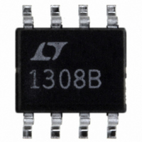
LT1308BCS8#TRPBF Linear Technology, LT1308BCS8#TRPBF Datasheet - Page 11

LT1308BCS8#TRPBF
Manufacturer Part Number
LT1308BCS8#TRPBF
Description
IC DC/DC CONV SINGLE CELL 8-SOIC
Manufacturer
Linear Technology
Type
Step-Up (Boost)r
Datasheet
1.LT1308ACS8PBF.pdf
(20 pages)
Specifications of LT1308BCS8#TRPBF
Internal Switch(s)
Yes
Synchronous Rectifier
No
Number Of Outputs
1
Voltage - Output
5V
Current - Output
1A
Frequency - Switching
600kHz
Voltage - Input
1 ~ 10 V
Operating Temperature
0°C ~ 70°C
Mounting Type
Surface Mount
Package / Case
8-SOIC (3.9mm Width)
Lead Free Status / RoHS Status
Lead free / RoHS Compliant
Power - Output
-
Available stocks
Company
Part Number
Manufacturer
Quantity
Price
APPLICATIONS INFORMATION
SHDN PIN
The LT1308A/LT1308B SHDN pin is improved over the
LT1308. The pin does not require tying to V
the device, but needs only a logic level signal. The voltage
on the SHDN pin can vary from 1V to 10V independent
of V
grounding, which is to shut the device down, reducing
current drain to 1μA or less.
LOW-BATTERY DETECTOR
The low-battery detector on the LT1308A/LT1308B fea-
tures improved accuracy and drive capability compared
to the LT1308. The 200mV reference has an accuracy of
± 2% and the open-collector output can sink 50μA. The
LT1308A/LT1308B low-battery detector is a simple PNP
input gain stage with an open-collector NPN output. The
negative input of the gain stage is tied internally to a 200mV
reference. The positive input is the LBI pin. Arrangement as
a low-battery detector is straightforward. Figure 10 details
hookup. R1 and R2 need only be low enough in value so
that the bias current of the LBI pin doesn’t cause large
errors. For R2, 100k is adequate. The 200mV reference
can also be accessed as shown in Figure 11.
V
BAT
IN
V
. Further, fl oating this pin has the same effect as
Figure 10. Setting Low-Battery Detector Trip Point
BAT
R1
R2
100k
Figure 11. Accessing 200mV Reference
200mV
V
REF
2N3906
LBI
GND
10k
200mV
INTERNAL
REFERENCE
+
–
+
V
IN
200k
10μF
LT1308A
LT1308B
LBO
1308 F10
LBO
LBI
LT1308A
LT1308B
GND
V
5V
IN
1308 F11
100k
R1 =
IN
TO PROCESSOR
V
LB
to enable
– 200mV
2μA
A cross plot of the low-battery detector is shown in
Figure 12. The LBI pin is swept with an input which var-
ies from 195mV to 205mV, and LBO (with a 100k pull-up
resistor) is displayed.
START-UP
The LT1308A/LT1308B can start up into heavy loads, unlike
many CMOS DC/DC converters that derive operating voltage
from the output (a technique known as “bootstrapping”).
Figure 13 details start-up waveforms of Figure 1’s circuit
with a 20Ω load and V
3.5A as the output capacitor is charged. After the output
reaches 5V, inductor current is about 1A. In Figure 14, the
load is 5Ω and input voltage is 3V. Output voltage reaches
5V in 500μs after the device is enabled. Figure 15 shows
start-up behavior of Figure 5’s SEPIC circuit, driven from a
9V input with a 10Ω load. The output reaches 5V in about
1ms after the device is enabled.
2V/DIV
1A/DIV
5V/DIV
1V/DIV
V
V
SHDN
V
OUT
LBO
I
L1
Figure 13. 5V Boost Converter of Figure 1.
Start-Up from 1.5V Input into 20Ω Load
195
Figure 12. Low-Battery Detector
Input/Output Characteristic
LT1308A/LT1308B
IN
of 1.5V. Inductor current rises to
1ms/DIV
V
LBI
200
(mV)
1308 F13
1308 F12
205
11
1308abfb


