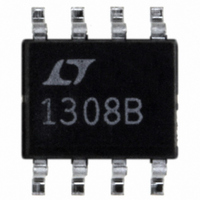
LT1308BCS8#TRPBF Linear Technology, LT1308BCS8#TRPBF Datasheet - Page 6

LT1308BCS8#TRPBF
Manufacturer Part Number
LT1308BCS8#TRPBF
Description
IC DC/DC CONV SINGLE CELL 8-SOIC
Manufacturer
Linear Technology
Type
Step-Up (Boost)r
Datasheet
1.LT1308ACS8PBF.pdf
(20 pages)
Specifications of LT1308BCS8#TRPBF
Internal Switch(s)
Yes
Synchronous Rectifier
No
Number Of Outputs
1
Voltage - Output
5V
Current - Output
1A
Frequency - Switching
600kHz
Voltage - Input
1 ~ 10 V
Operating Temperature
0°C ~ 70°C
Mounting Type
Surface Mount
Package / Case
8-SOIC (3.9mm Width)
Lead Free Status / RoHS Status
Lead free / RoHS Compliant
Power - Output
-
Available stocks
Company
Part Number
Manufacturer
Quantity
Price
PIN FUNCTIONS
LT1308A/LT1308B
V
Connect a series RC from this pin to ground. Typical values
are 47kΩ and 100pF. Minimize trace area at V
FB (Pin 2/Pin 2): Feedback Pin. Reference voltage is
1.22V. Connect resistive divider tap here. Minimize trace
area at FB. Set V
SHDN (Pin 3/Pin 3): Shutdown. Ground this pin to turn
off switcher. To enable, tie to 1V or more. SHDN does
not need to be at V
GND (Pin 4/Pins 4, 5, 6, 7): Ground. Connect directly
to local ground plane. Ground plane should enclose all
components associated with the LT1308. PCB copper
connected to these pins also functions as a heat sink. For
the TSSOP package, connect all pins to ground copper
to get the best heat transfer. This keeps chip heating to
a minimum.
6
C
V
(Pin 1/Pin 1): Compensation Pin for Error Amplifi er.
OUT
= 1.22V(1 + R1/R2).
OUT
IN
according to:
to enable the device.
(SO/TSSOP)
C
.
SW (Pin 5/Pins 8, 9, 10): Switch Pins. Connect induc-
tor/diode here. Minimize trace area at these pins to keep
EMI down. For the TSSOP package, connect all SW pins
together at the package.
V
bypass capacitor right at the pins, connected directly to
ground. For the TSSOP package, connect both V
together at the package.
LBI (Pin 7/Pin 13): Low-Battery Detector Input. 200mV
reference. Voltage on LBI must stay between –100mV
and 1V. Low-battery detector does not function with
SHDN pin grounded. Float LBI pin if not used.
LBO (Pin 8/Pin 14): Low-Battery Detector Output. Open
collector, can sink 50μA. A 220kΩ pull-up is recommend-
ed. LBO is high impedance when SHDN is grounded.
IN
(Pin 6/Pins 11, 12): Supply Pins. Must have local
IN
1308abfb
pins


