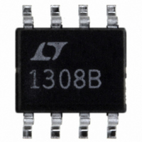
LT1308BCS8#TRPBF Linear Technology, LT1308BCS8#TRPBF Datasheet - Page 8

LT1308BCS8#TRPBF
Manufacturer Part Number
LT1308BCS8#TRPBF
Description
IC DC/DC CONV SINGLE CELL 8-SOIC
Manufacturer
Linear Technology
Type
Step-Up (Boost)r
Datasheet
1.LT1308ACS8PBF.pdf
(20 pages)
Specifications of LT1308BCS8#TRPBF
Internal Switch(s)
Yes
Synchronous Rectifier
No
Number Of Outputs
1
Voltage - Output
5V
Current - Output
1A
Frequency - Switching
600kHz
Voltage - Input
1 ~ 10 V
Operating Temperature
0°C ~ 70°C
Mounting Type
Surface Mount
Package / Case
8-SOIC (3.9mm Width)
Lead Free Status / RoHS Status
Lead free / RoHS Compliant
Power - Output
-
Available stocks
Company
Part Number
Manufacturer
Quantity
Price
APPLICATIONS INFORMATION
LT1308A/LT1308B
OPERATION
The LT1308A combines a current mode, fi xed frequency
PWM architecture with Burst Mode micropower opera-
tion to maintain high effi ciency at light loads. Operation
can be best understood by referring to the block diagram
in Figure 2. Q1 and Q2 form a bandgap reference core
whose loop is closed around the output of the converter.
When V
an 80mV drop across R5 and R6, forward biases Q1 and
Q2’s base collector junctions to 300mV. Because this is not
enough to saturate either transistor, FB can be at a higher
voltage than V
above 1.22V, causing V
decrease. When V
etic comparator A1, A1’s output goes low, turning off
all circuitry except the input stage, error amplifi er and
low-battery detector. Total current consumption in this
state is 140μA. As output loading causes the FB voltage to
decrease, A1’s output goes high, enabling the rest of the IC.
Switch current is limited to approximately 400mA initially
after A1’s output goes high. If the load is light, the output
voltage (and FB voltage) will increase until A1’s output goes
low, turning off the rest of the LT1308A. Low frequency
ripple voltage appears at the output. The ripple frequency
is dependent on load current and output capacitance.
This Burst Mode operation keeps the output regulated
and reduces average current into the IC, resulting in high
effi ciency even at load currents of 1mA or less.
If the output load increases suffi ciently, A1’s output
remains high, resulting in continuous operation. When the
LT1308A is running continuously, peak switch current is
controlled by V
is turned on at the beginning of each switch cycle. When
the summation of a signal representing switch current
and a ramp generator (introduced to avoid subharmonic
oscillations at duty factors greater than 50%) exceeds the
V
fl op and turning off the switch. Output voltage increases
as switch current is increased. The output, attenuated
by a resistor divider, appears at the FB pin, closing the
overall loop. Frequency compensation is provided by an
external series RC network connected between the V
and ground.
8
C
signal, comparator A2 changes state, resetting the fl ip-
IN
is 1V, the feedback voltage of 1.22V, along with
IN
C
. When there is no load, FB rises slightly
to regulate the output voltage. The switch
C
reaches the bias voltage on hyster-
C
(the error amplifi er’s output) to
C
pin
Low-battery detector A4’s open-collector output (LBO)
pulls low when the LBI pin voltage drops below 200mV.
There is no hysteresis in A4, allowing it to be used as an
amplifi er in some applications. The entire device is disabled
when the SHDN pin is brought low. To enable the converter,
SHDN must be at 1V or greater. It need not be tied to V
as on the LT1308.
The LT1308B differs from the LT1308A in that there is no
hysteresis in comparator A1. Also, the bias point on A1 is
set lower than on the LT1308B so that switching can occur
at inductor current less than 100mA. Because A1 has no
hysteresis, there is no Burst Mode operation at light loads
and the device continues switching at constant frequency.
This results in the absence of low frequency output voltage
ripple at the expense of effi ciency.
The difference between the two devices is clearly illus-
trated in Figure 3. The top two traces in Figure 3 shows an
LT1308A/LT1308B circuit, using the components indicated
in Figure 1, set to a 5V output. Input voltage is 3V. Load
current is stepped from 50mA to 800mA for both circuits.
Low frequency Burst Mode operation voltage ripple is
observed on Trace A, while none is observed on Trace B.
At light loads, the LT1308B will begin to skip alternate cycles.
The load point at which this occurs can be decreased by
increasing the inductor value. However, output ripple will
continue to be signifi cantly less than the LT1308A output
ripple. Further, the LT1308B can be forced into micropower
mode, where I
or more out of the V
A1’s output to go low.
TRACE A: LT1308A
TRACE B: LT1308B
V
V
OUT
OUT
I
LOAD
AC COUPLED
AC COUPLED
Figure 3. LT1308A Exhibits Burst Mode Operation Output
Voltage Ripple at 50mA Load, LT1308B Does Not
, 100mV/DIV
, 100mV/DIV
800mA
50mA
V
(CIRCUIT OF FIGURE 1)
Q
IN
falls from 3mA to 200μA by sinking 40μA
= 3V
C
pin. This stops switching by causing
200μs/DIV
1308 F03
1308abfb
IN


