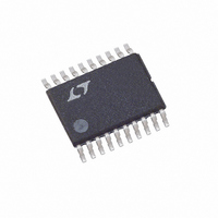
LTC3417AIFE-2#TRPBF Linear Technology, LTC3417AIFE-2#TRPBF Datasheet

LTC3417AIFE-2#TRPBF
Specifications of LTC3417AIFE-2#TRPBF
Available stocks
Related parts for LTC3417AIFE-2#TRPBF
LTC3417AIFE-2#TRPBF Summary of contents
Page 1
... In shutdown, the device draws <1μA. L, LT, LTC, LTM and Burst Mode are registered trademarks of Linear Technology Corporation. All other trademarks are the property of their respective owners. Protected by U.S. Patents including 5481178, 6580258, 6304066, 6127815, 6498466, 6611131, 6144194. ...
Page 2
... LTC3417AEFE-2#PBF LTC3417AEFE-2#TRPBF LTC3417AIFE-2#PBF LTC3417AIFE-2#TRPBF Consult LTC Marketing for parts specifi ed with wider operating temperature ranges. *The temperature grade is identifi label on the shipping container. Consult LTC Marketing for information on non-standard lead based fi nish parts. For more information on lead free part marking, go to: For more information on tape and reel specifi ...
Page 3
ELECTRICAL CHARACTERISTICS temperature range, otherwise specifi cations are at T SYMBOL PARAMETER Operating Voltage Range IN1 IN2 Feedback Pin Input Current FB1 FB2 Feedback Voltage FB1 FB2 ΔV Reference Voltage Line ...
Page 4
LTC3417A-2 ELECTRICAL CHARACTERISTICS Note 1: Stresses beyond those listed under Absolute Maximum Ratings may cause permanent damage to the device. Exposure to any Absolute Maximum Rating condition for extended periods may affect device reliability and lifetime. Note 2: The LTC3417AE-2 ...
Page 5
TYPICAL PERFORMANCE CHARACTERISTICS OUT1 Effi ciency vs Load Current 100 1.8V OUT Burst Mode OPERATION 70 PULSE SKIP FORCED 65 CONTINUOUS REFER TO FIGURE 4 60 0.001 0.01 0.1 ...
Page 6
LTC3417A-2 TYPICAL PERFORMANCE CHARACTERISTICS OUT2 DS(ON 27°C A 0.19 P-CHANNEL SWITCH 0.18 0.17 0.16 0.15 N-CHANNEL SWITCH 0. 2.5 3 3.5 4.5 V (V) IN 3417A-2 G16 PIN FUNCTIONS (DFN/TSSOP) ...
Page 7
PIN FUNCTIONS ( DFN/ TSSOP the 1.5A regulator and the 1A regulator are in phase. IN When PHASE is at 0V, the 1.5A regulator and the 1A regulator are switching 180 degrees out-of-phase. Do not fl oat this ...
Page 8
LTC3417A-2 OPERATION The LTC3417A-2 uses a constant frequency, current mode architecture. Both channels share the same clock frequency. The PHASE pin sets whether the channels are running in-phase or out of phase. The operating frequency is determined by connecting the ...
Page 9
APPLICATIONS INFORMATION A general LTC3417A-2 application circuit is shown in Figure 4. External component selection is driven by the load requirement, and begins with the selection of the inductors L1 and L2. Once L1 and L2 are chosen ...
Page 10
LTC3417A-2 APPLICATIONS INFORMATION The inductor value will also have an effect on Burst Mode operation. The transition from low current operation begins when the peak inductor current falls below a level set by the burst clamp. Lower inductor values result ...
Page 11
APPLICATIONS INFORMATION When then the equation simplifi 1– RMS – V OUT IN OUT ( ) ...
Page 12
LTC3417A-2 APPLICATIONS INFORMATION is given to ripple current ratings and long term reliability. Ceramic capacitors have the lowest ESR and cost but also have the lowest capacitance density, high voltage and temperature coeffi cient and exhibit audible piezoelectric effects. In ...
Page 13
APPLICATIONS INFORMATION V RUN 2V/DIV V OUT 1V/DIV I L 1A/DIV V = 3.6V 200μs/DIV 1.8V OUT R = 0.9Ω L Figure 2. Digital Soft-Start OUT1 Soft-Start Soft-start reduces surge currents from V ally increasing the peak ...
Page 14
... Percent effi ciency can be expressed as: % Effi ciency = 100% – (P1 +…) where P1, P2, etc. are the individual losses as a percent- age of input power. Hot Swap is a trademark of Linear Technology Corporation. drops toward V , the load step capability OUT , causing a rapid drop in V ...
Page 15
APPLICATIONS INFORMATION Although all dissipative elements in the circuit produce losses, four main sources account for most of the losses in LTC3417A-2 circuits: 1) LTC3417A switching losses losses, 4) other losses. 1) The I current ...
Page 16
LTC3417A-2 APPLICATIONS INFORMATION The power dissipated by the part is • • DS(ON)1 2 DS(ON 1.5 • 0. • 0.163 PD = 366mW The ...
Page 17
APPLICATIONS INFORMATION V IN 2.25V TO 5.5V V OUT1 1.8V C1 22pF 1.5A R1 511k C OUT1 47μF L1: MIDCOM DUS-5121-1R5R C : KEMET C1210C226K8PAC OUT1 IN1 IN2 10μF 0.1μF 0.1μ IN1 IN2 L1 ...
Page 18
LTC3417A-2 APPLICATIONS INFORMATION Board Layout Considerations When laying out the printed circuit board, the following checklist should be used to ensure proper operation of the LTC3417A-2. These items are also illustrated graphically in the layout diagram of Figure 5. Check ...
Page 19
... DIMENSIONS ARE IN 3. DRAWING NOT TO SCALE Information furnished by Linear Technology Corporation is believed to be accurate and reliable. However, no responsibility is assumed for its use. Linear Technology Corporation makes no representa- tion that the interconnection of its circuits as described herein will not infringe on existing patent rights. DHC Package 16-Lead Plastic DFN (5mm × ...
Page 20
... Converter LTC3561 1.25A, 4MHz, Synchronous Step-Down DC/DC Converter 2 LTC3562 Quad Interface, 600/600/400/400mA , 2.25MHz Synchronous Step-Down DC/DC Converter ThinSOT is a trademark of Linear Technology Corporation. 20 Linear Technology Corporation 1630 McCarthy Blvd., Milpitas, CA 95035-7417 (408) 432-1900 FAX: (408) 434-0507 ● COMMENTS 96% Effi ciency 20μ ...


