ADP2102YCPZ-1.8-R7 Analog Devices Inc, ADP2102YCPZ-1.8-R7 Datasheet
ADP2102YCPZ-1.8-R7
Specifications of ADP2102YCPZ-1.8-R7


Related parts for ADP2102YCPZ-1.8-R7


ADP2102YCPZ-1.8-R7 Summary of contents
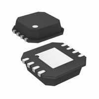
Page 1
FEATURES Input voltage range: 2 5.5 V 600 mA maximum load current 95% efficiency Low duty cycle operation Only 3 tiny external ceramic components 3 MHz typical operating frequency Fixed output voltage from 0 1.875 V ...
Page 2
ADP2102 TABLE OF CONTENTS Features .............................................................................................. 1 Applications....................................................................................... 1 General Description ......................................................................... 1 Typical Performance Characteristics ............................................. 1 Typical Applications Circuit............................................................ 1 Revision History ............................................................................... 2 Specifications..................................................................................... 3 Absolute Maximum Ratings............................................................ 4 Thermal Resistance ...................................................................... 4 Boundary Condition.................................................................... 4 ESD ...
Page 3
SPECIFICATIONS MODE = Table 1. Parameter Conditions INPUT CHARACTERISTICS 2 Input Voltage Range Undervoltage Lockout Threshold V Undervoltage Lockout Hysteresis OUTPUT CHARACTERISTICS Output Voltage Range ...
Page 4
ADP2102 ABSOLUTE MAXIMUM RATINGS Table 2. Parameter AVIN, EN, MODE, FB/OUT to AGND LX to PGND PVIN to PGND PGND to AGND AVIN to PVIN Operating Ambient Temperature Range Junction Temperature Range Storage Temperature Range Soldering Conditions 1 The ADP2102 ...
Page 5
PIN CONFIGURATION AND FUNCTION DESCRIPTIONS Table 4. Pin Function Descriptions Pin No. Mnemonic Description 1 MODE Mode Input. To set the ADP2102 to forced continuous conduction mode (CCM), drive MODE high. To set the ADP2102 to power save mode/auto mode ...
Page 6
ADP2102 TYPICAL PERFORMANCE CHARACTERISTICS 2.2 μ 2.2 μ OUT 100 2. 3. LOAD ...
Page 7
100 LOAD CURRENT (mA) Figure 10. Efficiency vs. Load Current (V OUT 95 PSM CCM 65 ...
Page 8
ADP2102 1.52 1.51 1. 0mA LOAD I = 300mA 1.49 LOAD I = 600mA LOAD 1.48 1.47 1.46 –40 – TEMPERATURE (°C) Figure 16. Output Voltage vs. Temperature (V 1. 0mA LOAD I = ...
Page 9
LOAD CURRENT (mA) Figure 22. Switching Frequency vs. Load Current 1.08 1.07 1.06 1.05 1.04 1.03 1.02 1.01 1.00 2.7 3.0 ...
Page 10
ADP2102 T CH4 CH1 CH2: V OUT 2 CH1 500mA Ω CH2 2.00V M 10.0µ CH4 2.00V 51.00% Figure 28. PSM Mode Operation at Light Loads (75 mA) T ...
Page 11
T CH1: V (AC) OUT 1 CH2: I (0mA TO 300mA) LOAD 2 CH1 50.0mV CH2 200mA Ω M 100µs A CH2 –300.000µs Figure 34. Load Transient Response (V OUT T CH1: V (AC) OUT 1 CH3: ...
Page 12
ADP2102 T CH1 CH2: V OUT 2 CH3 CH1 2.00V CH2 500mV M 2.00ms A CH2 CH3 200mA Ω 6.600% Figure 40. Heavy Load Start-Up Waveform T CH4: V ...
Page 13
THEORY OF OPERATION The ADP2102 is a high frequency, synchronous step-down, dc-to-dc converter optimized for battery-powered, portable applications based on constant on-time current-mode control architecture with voltage feed forward to null frequency variation with line voltage, creating a ...
Page 14
ADP2102 As a result of this auto mode control technique, losses are minimized at light loads, improving system efficiency. The PSM reverse current comparator controls the entry and exit into forced continuous conduction mode. Some minor jitter is normal during ...
Page 15
SOFT START The ADP2102 has an internal soft start function that ramps the output voltage in a controlled manner upon startup, therefore limiting the inrush current. This prevents possible input voltage drops when a battery or a high impedance power ...
Page 16
ADP2102 APPLICATIONS INFORMATION The external component selection for the ADP2102 applications circuit, as shown in Figure 2, is driven by the load requirement and begins with the selection of Inductor L. Once the inductor is chosen, C and C can ...
Page 17
Table 5. Recommended Inductor Selection Manufacturer Series FDK Corporation MIPF2520D TDK MLP2520S2R2L Murata LQM2HPN2R2MJ0 Coilcraft, Inc. LPS3015-222ML Taiyo Yuden NR3010T2R2M Table 6. Recommended Input and Output Capacitor Selection Capacitor Murata 2.2 μF 6.3 V GRM188R60J225K X5R 0603 4.7 μF 6.3 ...
Page 18
ADP2102 ADP2102-ADJ 1 MODE FB/OUT 4 AGND C R2 ADP2102-ADJ 8 MODE AVIN 7 EN PVIN L1 6 FB/OUT LX 2.2µH 5 AGND PGND C C OUT IN 4.7µF 2.2µ ...
Page 19
SETTING THE OUTPUT VOLTAGE The output voltage of the ADP2102-ADJ is externally set by a resistive voltage divider from the output voltage to FB. The ratio of the resistive voltage divider sets the output voltage, and the absolute value of ...
Page 20
ADP2102 Inductor Losses Inductor conduction losses are caused by the flow of current through the inductor, which has an internal resistance (DCR) associated with it. Larger sized inductors have smaller DCR, which may decrease inductor conduction losses. Inductor core losses ...
Page 21
Output Capacitor For transient applications, assume a droop of 0.1 V. Typically, it takes two to three cycles for the output to settle from a load transient because the capacitor alone supplies the load current until the loop responds. Under ...
Page 22
ADP2102 CIRCUIT BOARD LAYOUT RECOMMENDATIONS Good circuit board layout is essential in obtaining the best performance from the ADP2102. Poor circuit layout degrades the output ripple and regulation, as well as the EMI and electromagnetic compatibility performance. Figure 52 and ...
Page 23
VIN MODE CBP EN FB/OUT ADP2102 AGND Figure 52. Recommended Layout of the Top Layer of the ADP2102-FXD Application Board VIN MODE EN AGND FB/OUT Figure 53. Recommended Layout of the Bottom Layer of the ADP2102-FXD Application Board Rev. B ...
Page 24
... MAX 0.85 NOM SEATING PLANE ORDERING GUIDE Output Model Current (mA) 1 ADP2102YCPZ-0.8-R7 600 1 ADP2102YCPZ-1.0-R7 600 1 ADP2102YCPZ-1.2-R7 600 1 ADP2102YCPZ-1.25R7 600 1 ADP2102YCPZ-1.37R7 600 ADP2102YCPZ-1.5-R7 1 600 1 ADP2102YCPZ-1.8-R7 600 ADP2102YCPZ-1.87R7 1 600 1 ADP2102YCPZ-1-R7 600 1 ADP2102YCPZ-2-R7 600 1 ADP2102YCPZ-3-R7 600 1 ADP2102YCPZ-4-R7 600 1 ADP2102-0.8-EVALZ 1 ADP2102-1.0-EVALZ 1 ADP2102-1.2-EVALZ 1 ADP2102-1.25-EVALZ 1 ADP2102-1.375-EVALZ 1 ADP2102-1 ...