L6726A STMicroelectronics, L6726A Datasheet - Page 18

L6726A
Manufacturer Part Number
L6726A
Description
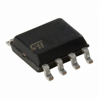
IC CTRLR PWM 1PHASE SO-8
Manufacturer
STMicroelectronics
Type
Step-Down (Buck)r
Datasheet
1.L6726ATR.pdf
(35 pages)
Specifications of L6726A
Internal Switch(s)
No
Synchronous Rectifier
No
Number Of Outputs
1
Voltage - Output
Adj to 0.8V
Frequency - Switching
270kHz
Voltage - Input
1.5 ~ 12 V
Operating Temperature
-20°C ~ 85°C
Mounting Type
Surface Mount
Package / Case
8-SOIC (3.9mm Width)
Output Current
1.5 A
Input Voltage
4.1 V to 13.2 V
Operating Temperature Range
- 40 C to + 150 C
Mounting Style
SMD/SMT
For Use With
497-9046 - BOARD EVAL BASED ON L6726A497-6364 - BOARD DEMO FOR TS4995EIJT497-6259 - BOARD EVAL 1PH STPDN CONV L6726A
Lead Free Status / RoHS Status
Lead free / RoHS Compliant
Current - Output
-
Power - Output
-
Lead Free Status / Rohs Status
Lead free / RoHS Compliant
Available stocks
Company
Part Number
Manufacturer
Quantity
Price
Part Number:
L6726A
Manufacturer:
ST
Quantity:
20 000
Part Number:
L6726AD
Manufacturer:
ST
Quantity:
20 000
Company:
Part Number:
L6726ATR
Manufacturer:
FUJI
Quantity:
130
Part Number:
L6726ATR
Manufacturer:
ST
Quantity:
20 000
Application details
8.3
8.4
18/35
Soft-start time calculation
To calculate SS time (t
The previous equation refers only to V
OC setting phase or COMP set free to the beginning of V
approximately estimated as follow:
Once calculated t
output capacitor bank can be estimated:
Layout guidelines
L6726A provides control functions and high current integrated drivers to implement high-
current step-down DC-DC converters. In this kind of application, a good layout is very
important.
The first priority when placing components for these applications has to be reserved to the
power section, minimizing the length of each connection and loop as much as possible. To
minimize noise and voltage spikes (EMI and losses) power connections (highlighted in
Figure
traces: loop must be anyway minimized. The critical components, i.e. the power MOSFETs,
must be close one to the other. The use of multi-layer printed circuit board is recommended.
Figure 10. Power connections (heavy lines)
The input capacitance (C
placed close to the power section in order to eliminate the stray inductance generated by the
copper traces. Low ESR and ESL capacitors are preferred, MLCC are suggested to be
connected near the HS drain.
Use proper number of vias when power traces have to move between different planes on the
PCB in order to reduce both parasitic resistance and inductance. Moreover, reproducing the
same high-current trace on more than one PCB layer will reduce the parasitic resistance
associated to that connection.
10) must be a part of a power plane and anyway realized by wide and thick copper
t
delay
I
t
startup
SS
SS
=
=
, also the current delivered by the converter during SS to charge the
C
------------------------------------------------- -
=
L6726A
C
----------------------- -
F
SS
F
C
--------------------------------- -
⋅
I
⋅
V
-------------- ΔV
SS
OUT
UGATE
PHASE
), the following approximated equation can be used (C
LGATE
0.8V
GND
IN
V
OUT
IN
), or at least a portion of the total capacitance needed, has to be
I
t
SS
SS
⋅
V
⋅
Doc ID 12754 Rev 4
OUT
OSC
OUT
ramp up time. The time elapsed from the end of
C
V
IN
IN
L
OUT
C
OUT
ramp up (see
LOAD
Figure
P
<<C
6) can be
L6726A
F
):


