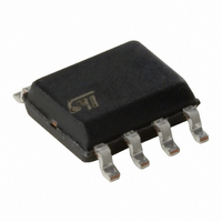
L6726A STMicroelectronics, L6726A Datasheet - Page 21

L6726A
Manufacturer Part Number
L6726A
Description
IC CTRLR PWM 1PHASE SO-8
Manufacturer
STMicroelectronics
Type
Step-Down (Buck)r
Datasheet
1.L6726ATR.pdf
(35 pages)
Specifications of L6726A
Internal Switch(s)
No
Synchronous Rectifier
No
Number Of Outputs
1
Voltage - Output
Adj to 0.8V
Frequency - Switching
270kHz
Voltage - Input
1.5 ~ 12 V
Operating Temperature
-20°C ~ 85°C
Mounting Type
Surface Mount
Package / Case
8-SOIC (3.9mm Width)
Output Current
1.5 A
Input Voltage
4.1 V to 13.2 V
Operating Temperature Range
- 40 C to + 150 C
Mounting Style
SMD/SMT
For Use With
497-9046 - BOARD EVAL BASED ON L6726A497-6364 - BOARD DEMO FOR TS4995EIJT497-6259 - BOARD EVAL 1PH STPDN CONV L6726A
Lead Free Status / RoHS Status
Lead free / RoHS Compliant
Current - Output
-
Power - Output
-
Lead Free Status / Rohs Status
Lead free / RoHS Compliant
Available stocks
Company
Part Number
Manufacturer
Quantity
Price
Part Number:
L6726A
Manufacturer:
ST
Quantity:
20 000
Part Number:
L6726AD
Manufacturer:
ST
Quantity:
20 000
Company:
Part Number:
L6726ATR
Manufacturer:
FUJI
Quantity:
130
Part Number:
L6726ATR
Manufacturer:
ST
Quantity:
20 000
L6726A
9
9.1
Application Information
Output inductor
Inductor value is defined by a compromise between dynamic response, ripple, efficiency,
cost and size. Usually, inductance is calculated to maintain inductor ripple current (ΔI
between 20% and 30% of maximum output current. Given the switching frequency (F
the input voltage (V
inductance can be calculated as follows:
Figure 12
V
Increasing inductance reduces inductor ripple current (and output voltage ripple
accordingly) but, at the same time, increases the converter response time to load transients.
Higher inductance means that the inductor needs more time to change its current from initial
to final value. Until the inductor has not finished its charging, the additional output current is
supplied by output capacitors. Minimizing the response time lead to minimize the output
capacitance required. If the compensation network is designed with high bandwidth, during
an heavy load transient the device is able to saturate duty cycle (0% or 80%). When this
condition is reached, the response time is limited only by the time required to charge the
inductor.
Figure 12. Inductor current ripple vs output voltage
L
IN
=
= 5 V and V
V
----------------------------- -
]
[ A
l e
p
p
r i
t
n
e
r r
u
c
r
t o
c
u
d
I n
F
IN
SW
12
10
–
8
6
4
2
0
V
⋅
shows the ripple current vs. the output voltage for different inductance, with
0
ΔI
OUT
L
⋅
IN
V
--------------
V
OUT
= 12 V.
IN
IN
), the output voltage (V
1
Ou tp u t vo ltag e [V ]
Doc ID 12754 Rev 4
2
OUT
3
) and the desired ripple current (ΔI
4
Application Information
5
Vin =1 2 V, L =1 u H
Vin =1 2 V, L =2 u H
Vin =5 V, L =5 0 0 n H
Vin =5 V, L =1 .5 u H
L
),
L
SW
)
21/35
),


