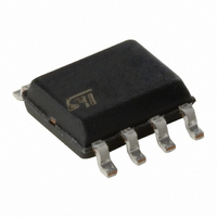
L6726A STMicroelectronics, L6726A Datasheet - Page 5

L6726A
Manufacturer Part Number
L6726A
Description
IC CTRLR PWM 1PHASE SO-8
Manufacturer
STMicroelectronics
Type
Step-Down (Buck)r
Datasheet
1.L6726ATR.pdf
(35 pages)
Specifications of L6726A
Internal Switch(s)
No
Synchronous Rectifier
No
Number Of Outputs
1
Voltage - Output
Adj to 0.8V
Frequency - Switching
270kHz
Voltage - Input
1.5 ~ 12 V
Operating Temperature
-20°C ~ 85°C
Mounting Type
Surface Mount
Package / Case
8-SOIC (3.9mm Width)
Output Current
1.5 A
Input Voltage
4.1 V to 13.2 V
Operating Temperature Range
- 40 C to + 150 C
Mounting Style
SMD/SMT
For Use With
497-9046 - BOARD EVAL BASED ON L6726A497-6364 - BOARD DEMO FOR TS4995EIJT497-6259 - BOARD EVAL 1PH STPDN CONV L6726A
Lead Free Status / RoHS Status
Lead free / RoHS Compliant
Current - Output
-
Power - Output
-
Lead Free Status / Rohs Status
Lead free / RoHS Compliant
Available stocks
Company
Part Number
Manufacturer
Quantity
Price
Part Number:
L6726A
Manufacturer:
ST
Quantity:
20 000
Part Number:
L6726AD
Manufacturer:
ST
Quantity:
20 000
Company:
Part Number:
L6726ATR
Manufacturer:
FUJI
Quantity:
130
Part Number:
L6726ATR
Manufacturer:
ST
Quantity:
20 000
L6726A
2
2.1
Pins description and connection diagrams
Figure 3.
Pin descriptions
Table 2.
Pin n
1
2
3
4
5
6
7
8
LGATE / OC
COMP / DIS
PHASE
UGATE
Pins connection (top view)
Pins descriptions
BOOT
Name
GND
VCC
FB
LGATE / OC
HS driver supply.
Connect through a capacitor (100 nF) to the floating node (LS-drain) pin
and provide necessary bootstrap diode from VCC.
HS driver output. Connect to HS MOSFET gate.
All internal references, logic and drivers are connected to this pin.
Connect to the PCB ground plane.
LGATE. LS driver output. Connect to LS MOSFET gate.
OC. Over current threshold set. During a short period of time following VCC
rising over UVLO threshold, a 10μA current is sourced from this pin.
Connect to GND with an R
Threshold. The resulting voltage at this pin is sampled and held internally
as the OC set point. Maximum programmable OC threshold is 0.55 V. A
voltage greater than 0.75V (max) activates an internal clamp and causes
OC threshold to be set at 400 mV. R
default threshold.
Device and LS driver power supply.
Operative range from 4.1 V to 13.2 V. Filter with at least 1μF MLCC to GND.
Error amplifier inverting input.
Connect with a resistor R
resistor R
reference.
COMP. Error amplifier output. Connect with an R
compensate the device control loop in conjunction to the FB pin.
During the soft-start phase, a 10 μA current is sourced from this pin so the
compensation capacitors also act to program the SS time.
DIS. The device can be disabled by pulling this pin lower than 0.4 V (min).
Setting free the pin, the device enables again.
HS driver return path, current-reading and adaptive-dead-time monitor.
Connect to the LS drain to sense R
This pin is also used by the adaptive-dead-time control circuitry to monitor
when HS MOSFET is OFF.
UGATE
BOOT
GND
Doc ID 12754 Rev 4
OS
to GND may be used to regulate voltages higher than the
1
2
3
4
L6726A
Pins description and connection diagrams
FB
OCSET
to the output regulated voltage. Additional
8
7
6
5
Function
resistor greater than 5kΩ to program OC
dsON
OCSET
PHASE
COMP / DIS
FB
VCC
drop to measure the output current.
not connected sets the 400 mV
F
- C
F
// C
P
to GND to
5/35


