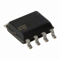
L6727 STMicroelectronics, L6727 Datasheet - Page 18

L6727
Manufacturer Part Number
L6727
Description
IC PWM CTLR SGL PHASE SO-8
Manufacturer
STMicroelectronics
Type
Step-Down (Buck)r
Datasheet
1.L6727TR.pdf
(34 pages)
Specifications of L6727
Internal Switch(s)
No
Synchronous Rectifier
No
Number Of Outputs
1
Voltage - Output
Adj to 0.8V
Frequency - Switching
300kHz
Voltage - Input
1.5 ~ 12 V
Operating Temperature
-20°C ~ 85°C
Mounting Type
Surface Mount
Package / Case
8-SOIC (3.9mm Width)
Output Current
1.5 A
Input Voltage
- 0.3 V to + 15 V
Switching Frequency
300 KHz
Operating Temperature Range
- 40 C to + 150 C
Mounting Style
SMD/SMT
Duty Cycle (max)
80 %
For Use With
497-8266 - BOARD EVAL BASED ON L6727497-6258 - BOARD EVAL 1PH STPDWN CONV L6727
Lead Free Status / RoHS Status
Lead free / RoHS Compliant
Current - Output
-
Power - Output
-
Lead Free Status / Rohs Status
Lead free / RoHS Compliant
Available stocks
Company
Part Number
Manufacturer
Quantity
Price
Part Number:
L6727
Manufacturer:
ST
Quantity:
20 000
Part Number:
L6727TR
Manufacturer:
ST
Quantity:
20 000
Application details
18/34
same high-current trace on more than one PCB layer will reduce the parasitic resistance
associated to that connection.
Connect output bulk capacitors (C
inductance and resistance associated to the copper trace, also adding extra decoupling
capacitors along the way to the load when this results in being far from the bulk capacitors
bank.
Figure 8.
Gate traces and phase trace must be sized according to the driver RMS current delivered to
the power MOSFET. The device robustness allows managing applications with the power
section far from the controller without losing performances. Anyway, when possible, it is
recommended to minimize the distance between controller and power section. See
for drivers current paths.
Small signal components and connections to critical nodes of the application, as well as
bypass capacitors for the device supply, are also important. Locate bypass capacitor (VCC
and Bootstrap capacitor) and loop compensation components as close to the device as
practical. For over current programmability, place R
leakage current paths on COMP / OC pin, since the internal current source is only 60μA.
Systems that do not use Schottky diode in parallel to the Low-Side MOSFET might show big
negative spikes on the phase pin. This spike must be limited within the absolute maximum
ratings (for example, adding a gate resistor in series to HS MOSFET gate, or a phase
resistor in series to PHASE pin), as well as the positive spike, but has an additional
consequence: it causes the bootstrap capacitor to be over-charged. This extra-charge can
cause, in the worst case condition of maximum input voltage and during particular
transients, that boot-to-phase voltage overcomes the absolute maximum ratings also
causing device failures. It is then suggested in this cases to limit this extra-charge by adding
a small resistor in series to the bootstrap diode (R
Figure 9.
LS DRIVER
LGATE
GND
VCC
Power connections (heavy lines)
Drivers turn-on and turn-off paths
R
GATE
L6727
LS MOSFET
R
UGATE
PHASE
LGATE
GND
INT
C
GS
C
GD
Doc ID 12933 Rev 4
OUT
) as near as possible to the load, minimizing parasitic
C
DS
V
C
IN
IN
D
HS DRIVER
OCSET
in
L
Figure
C
close to the device and avoid
PHASE
OUT
BOOT
UGATE
1).
R
PHASE
LOAD
R
GATE
HS MOSFET
R
INT
C
GS
C
GD
Figure 9
L6727
C
DS


