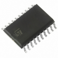
L4963D STMicroelectronics, L4963D Datasheet

L4963D
Specifications of L4963D
Available stocks
Related parts for L4963D
L4963D Summary of contents
Page 1
... This is advanced information on a new product now in development or underogin evaluation. Details are subject to change without notice. 1.5A SWITCHING REGULATOR Powerdip12+3+3 ORDERING NUMBERS: L4963W The L4963 is mounted in a 12+3+3 lead Powerdip (L4963) and SO20 large (L4963D) plastic pack- ages and requires very few external components. L4963 L4963D SO20 L4963D ...
Page 2
... L4963 - L4963D ABSOLUTE MAXIMUM RATINGS Symbol SO20 Powerdip – tot stg j P tot PIN CONNECTION (top view) 2/17 Parameter Input Voltage (pin 1 and pin 3 connected togheter) Input to Output Voltage Difference Negative Output DC Voltage Negative Output Peak Voltage at t=0.2 s, f=50kHz Power Fail Input ...
Page 3
... Oscillator waveform. A capacitor connected C OSCILLATOR between this terminal and ground modifies the maximum oscillator frequency. A resistor connected between this terminal and R OSCILLATOR FREQ. ground defines the maximum switching frequency. Parameter max. max. L4963 - L4963D Description SO20 Powerdip Unit C/W ...
Page 4
... L4963 - L4963D CIRCUIT DESCRIPTION (Refer to Block Dia- gram) The L4963 is a monolithic stepdown regulator pro- viding 1.5A at 5.1V working in discontinuous vari- able frequency mode. In normal operation the device resonates at a frequency depending primar- ily on the inductance value, the input and output voltage and the load current ...
Page 5
... 46V < I < 5mA 125 46V 5mA 65 ref V = 46V R = 51K 69 i osc ref 145 V = 46V 0mA ref 46V 0 46V 0. L4963 - L4963D = 25 C unless otherwise specified ) Typ. Max. Unit Fig 5 5.1 5.2 V 0.4 mV 150 0 100 ...
Page 6
... L4963 - L4963D ELECTRICAL CHARACTERISTIC (Continued) Symbol Parameter RESET V Rising Threshold Voltage 12 V Falling Threshold Voltage 12 Delay Rising Thereshold V 9D Voltage Delay Falling Thereshold V 9F Voltage –I Delay Source Current 9SO I Delay Sink Current 9SI I Output Leakage Current 10 V Output Saturation Volt. ...
Page 7
... Figure 2: Test Circuit Figure 3: DC Test Circuit Figure 3a Figure 3b L4963 - L4963D 7/17 ...
Page 8
... L4963 - L4963D Figure 3c Figure 4: Quiescent Drain Current vs. Supply Voltage (0% Duty Cycle) Figure 6: Quiescent Drain Current vs. Junction Temperature (0% Duty Cycle) 8/17 Figure 5: Quiescent Drain Current vs. Supply Voltage (100% Duty Cycle) Figure 7: Quiescent Drain Current vs. Junction Temperature (100% Duty Cycle) ...
Page 9
... Figure 8: Reference Voltage vs. V Figure 10: Line Transient Response Figure 12: Supply Voltage Ripple Rejection vs. Frequency Figure 9: Reference Voltage vs Figure 11: Load Transient Figure 13: Dropout Voltage Between pi3 and 2 L4963 - L4963D j vs. Current at pin2 9/17 ...
Page 10
... L4963 - L4963D Figure 14: Dropout Voltage Between pin3 and 2 vs. Junction Temperature Figure 16: Power Dissipation (device only) vs. In- put Voltage (Powerdip Package Only) Figure 18: Voltage and Current Waveform at pin2 10/17 Figure 15: Maximum Allowable PowerDissipation vs. Ambient Temperature (Powerdip Package Only) Figure 17: Power Dissipation (device only) vs. ...
Page 11
... Figure 20: Efficiency vs. Output Voltage (Power- dip Package Only) Figure 22: Current Limit vs. Input Voltage Figure 24: Oscillator Frequency vs. Junction Temperature Figure 21: Current Limit vs. Junction Tempera- ture V = 30V i Figure 23: Oscillator Frequency vs. R2 (see fig. 26) Figure 25: Oscillator Frequency vs. Input Voltage L4963 - L4963D 11/17 ...
Page 12
... L4963 - L4963D Figure 26: Evaluation Board Circuit PART LIST CAPACITOR C1 1000 F 50V EKR (*) C2 2.2mF 16V C3 1000 F 40V with low ESR 50V film RESISTOR 51K R5, R6 see table (*) Minimum 100 preregulated offline SMPS output or 1000 50Hz transformer plus rectifiers is used. i 12/17 Resistor Values for Standard Output Voltages ...
Page 13
... Figure 27: P.C. Board and Component Layout of the Circuit of fig. 26 (Powerdip Package) (1:1 scale). Figure 28: Thermal Characteristics Figure 29: Junction to Ambient Thermal Resis- tance vs. Area on Board Heatsink (SO20) L4963 - L4963D 13/17 ...
Page 14
... L4963 - L4963D Figure 30: A Minimal 5.1 Fixed Regulator — Very Few Components are Required Figure 31: A Minimal Components count for V 14/17 = 12V O ...
Page 15
... MAX. MIN. a1 0.51 0.020 B 0.85 1.40 0.033 b 0.50 b1 0.38 0.50 0.015 D 24.80 E 8.80 e 2.54 e3 20.32 F 7.10 I 5.10 L 3.30 Z 2.54 inch MECHANICAL DATA TYP. MAX. 0.055 0.020 0.020 0.976 0.346 0.100 0.800 0.280 0.201 0.130 0.100 L4963 - L4963D OUTLINE AND Powerdip 18 15/17 ...
Page 16
... L4963 - L4963D mm DIM. MIN. TYP. MAX. A 2.35 2.65 0.093 A1 0.1 0.3 0.004 B 0.33 0.51 0.013 C 0.23 0.32 0.009 D 12.6 13 0.496 E 7.4 7.6 0.291 e 1. 10.65 0.394 h 0.25 0.75 0.010 L 0.4 1.27 0.016 K 0˚ (min.)8˚ (max 16/17 inch MIN. TYP. ...
Page 17
... The ST logo is a registered trademark of STMicroelectronics © 2000 STMicroelectronics – Printed in Italy – All Rights Reserved Australia - Brazil - China - Finland - France - Germany - Hong Kong - India - Italy - Japan - Malaysia - Malta - Morocco - Singapore - Spain - Sweden - Switzerland - United Kingdom - U.S.A. STMicroelectronics GROUP OF COMPANIES http://www.st.com L4963 - L4963D 17/17 ...


