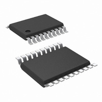
LM26420YMHX/NOPB National Semiconductor, LM26420YMHX/NOPB Datasheet - Page 15

LM26420YMHX/NOPB
Manufacturer Part Number
LM26420YMHX/NOPB
Description
IC REG DUAL SYNC BUCK 2A 20TSSOP
Manufacturer
National Semiconductor
Series
PowerWise®r
Type
Step-Down (Buck)r
Datasheet
1.LM26420XSQNOPB.pdf
(28 pages)
Specifications of LM26420YMHX/NOPB
Internal Switch(s)
Yes
Synchronous Rectifier
Yes
Number Of Outputs
2
Voltage - Output
0.8 ~ 4.5 V
Current - Output
2A
Frequency - Switching
550kHz
Voltage - Input
3 ~ 5.5 V
Operating Temperature
-40°C ~ 125°C
Mounting Type
Surface Mount
Package / Case
20-TSSOP Exposed Pad, 20-eTSSOP, 20-HTSSOP
Lead Free Status / RoHS Status
Lead free / RoHS Compliant
Power - Output
-
Other names
LM26420YMHX
Since the duty cycles of the two channels may overlap, cal-
culation of the input ripple RMS current is a little tedious. Use
the following equation.
I
maximum output current. d1 is the non-overlapping portion of
Channel 1's duty cycle D
of Channel 2's duty cycle D
the two duty cycles. I
I
d3, refer to the decision tree in . To determine the duty cycle
of each channel, use D = V
the following equation for a more accurate result.
OUTPUT CAPACITOR
The output capacitor is selected based upon the desired out-
put ripple and transient response. The initial current of a load
transient is provided mainly by the output capacitor. The out-
put ripple of the converter is:
When using MLCCs, the ESR is typically so low that the ca-
pacitive ripple may dominate. When this occurs, the output
ripple will be approximately sinusoidal and 90° phase shifted
from the switching action. Given the availability and quality of
MLCCs and the expected output voltage of designs using the
LM26420, there is really no need to review any other capacitor
technologies. Another benefit of ceramic capacitors is their
ability to bypass high frequency noise. A certain amount of
1
1
·D
is Channel 1's maximum output current. I
1
+ I
2
·D
2
. To quickly determine the values of d1, d2 and
av
1
is the average input current. I
. d2 is the non-overlapping portion
2
. d3 is the overlapping portion of
OUT
/V
IN
for a quick result or use
2
FIGURE 4. Determining d1, d2 and d3
is Channel 2's
av
=
15
R
resistance of the MOSFET switch.
Example:
V
R
input ripple RMS current equation, I
First, find out the duty cycles. Plug the numbers into the duty
cycle equation and we get D1 = 0.75, and D2 = 0.33. Next,
follow the decision tree in to find out the values of d1, d2 and
d3. In this case, d1 = 0.5, d2 = D2 + 0.5 - D1 = 0.08, and d3
= D1 - 0.5 = 0.25. I
the numbers into the input ripple RMS current equation and
the result is I
switching edge noise will couple through parasitic capaci-
tances in the inductor to the output. A ceramic capacitor will
bypass this noise while a tantalum will not. Since the output
capacitor is one of the two external components that control
the stability of the regulator control loop, most applications will
require a minimum of 22 µF of output capacitance. Capaci-
tance often, but not always, can be increased significantly
with little detriment to the regulator stability. Like the input ca-
pacitor, recommended multilayer ceramic capacitors are X7R
or X5R types.
PROGRAMMING OUTPUT VOLTAGE
The output voltage is set using the following equation where
R2 is connected between the FB pin and GND, and R1 is
connected between V
is 10kΩ. When designing a unity gain converter (V
R1 should be between 0Ω and 100Ω, and R2 should be on
the order of 5kΩ to 50kΩ, 10kΩ is the suggested value.
IN
DC
DS
= 5V, V
is the winding resistance of the inductor. R
= 170mΩ, R
OUT1
irrms
= 3.3V, I
= 0.77A.
DC
av
= 30mΩ. (I
= I
OUT
OUT1
OUT1
and the FB pin. A good value for R2
·D1 + I
= 2A, V
OUT1
OUT2
OUT2
OUT2
is the same as I
·D2 = 1.995A. Plug all
30069681
= 1.2V, I
is the same as I
DS
www.national.com
OUT2
OUT
is the ON
= 0.8V),
1
= 1.5A,
in the
2
).


