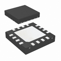
LM26420XSQX/NOPB National Semiconductor, LM26420XSQX/NOPB Datasheet - Page 18

LM26420XSQX/NOPB
Manufacturer Part Number
LM26420XSQX/NOPB
Description
IC REG DUAL SYNC BUCK 2A 16LLP
Manufacturer
National Semiconductor
Series
PowerWise®r
Type
Step-Down (Buck)r
Datasheet
1.LM26420XSQNOPB.pdf
(28 pages)
Specifications of LM26420XSQX/NOPB
Internal Switch(s)
Yes
Synchronous Rectifier
Yes
Number Of Outputs
2
Voltage - Output
0.8 ~ 4.5 V
Current - Output
2A
Frequency - Switching
2.2MHz
Voltage - Input
3 ~ 5.5 V
Operating Temperature
-40°C ~ 125°C
Mounting Type
Surface Mount
Package / Case
16-LLP
Lead Free Status / RoHS Status
Lead free / RoHS Compliant
Power - Output
-
Other names
LM26420XSQX
www.national.com
Calculating Efficiency, and Junction
Temperature
The complete LM26420 DC/DC converter efficiency can be
calculated in the following manner.
Or
Calculations for determining the most significant power loss-
es are shown below. Other losses totaling less than 2% are
not discussed.
Power loss (P
the converter: switching and conduction. Conduction losses
usually dominate at higher output loads, whereas switching
losses remain relatively fixed and dominate at lower output
loads. The first step in determining the losses is to calculate
the duty cycle (D):
V
is on, and is equal to:
V
is on, and is equal to:
If the voltage drop across the inductor (V
for, the equation becomes:
Another significant external power loss is the conduction loss
in the output inductor. The equation can be simplified to:
The LM26420 conduction loss is mainly associated with the
two internal FETs:
If the inductor ripple current is fairly small, the conduction
losses can be simplified to:
SW_TOP
SW_BOT
is the voltage drop across the internal PFET when it
is the voltage drop across the internal NFET when it
LOSS
V
V
SW_TOP
SW_BOT
) is the sum of two basic types of losses in
P
IND
= I
= I
= I
OUT
OUT
OUT
2
x R
x R
x R
DSON_TOP
DSON_BOT
DCR
DCR
) is accounted
18
Switching losses are also associated with the internal FETs.
They occur during the switch on and off transition periods,
where voltages and currents overlap resulting in power loss.
The simplest means to determine this loss is to empirically
measuring the rise and fall times (10% to 90%) of the switch
at the switch node.
Switching Power Loss is calculated as follows:
Another loss is the power required for operation of the internal
circuitry:
I
8.4mA (I
quency option.
Due to Dead-Time-Control Logic in the converter, there is a
small delay (~4nS) between the turn ON and OFF of the TOP
and BOTTOM FET. During this time, the body diode of the
BOTTOM FET is conducting with a voltage drop of V
(~.65V). This allows the inductor current to circulate to the
output, until the BOTTOM FET is turned ON an the inductor
current passes through the FET. There is a small amount of
power loss due to this body diode conducting and it can be
calculated as follows:
Typical Application power losses are:
These calculations assume a junction temperature of 25°C.
The R
therefore the internal power loss (P
culated to estimate the rise in junction temperature.
Q
is the quiescent operating current, and is typically around
R
R
DSON
P
P
V
DSON_TOP
DSON_BOT
IND
QVINC
LOSS
T
T
BDIODE
BDIODE
P
I
F
P
V
OUT
RISE
FALL
I
D
INTERNAL
SW
η
COND_BOT
Q
IN
DCR
values will be larger due to internal heating and
P
P
P
COND_TOP
SWR
SWF
P
= ΣP
= 4.7mA + I
COND
= 2x(V
= 1/2(V
Power Loss Tabulation
= 1/2(V
COND
= ΣP
P
= P
= (I
550kHz
8.4mA
SW
86.2%
0.65V
1.5nS
1.5nS
75mΩ
55mΩ
20mΩ
0.262
5.0V
2.0A
BDIODE
= (I
P
OUT
COND_TOP
+ P
COND
= P
IN
IN
Q
QVIND
OUT
= I
x I
2
x I
SW
SWR
x R
x I
Q
2
OUT
+ P
OUT
+ P
x R
=3.7mA) for the 550 kHz fre-
x V
OUT
DSON_BOT
+ P
P
P
SW
P
+ P
x F
x F
BDIODE
P
COND_TOP
COND_BOT
DSON_TOP
INTERNAL
IN
INTERNAL
P
P
P
V
P
BDIODE
+ P
x F
P
SWF
P
LOSS
SWR
SW
SW
OUT
OUT
SWF
COND_BOT
IND
Q
SW
BDIODE
x T
x T
+ P
x (1-D))
x T
) must be first cal-
RISE
FALL
x D)
IND
BDIODE
+ P
167mW
384mW
304mW
)
5.7mW
4.1mW
4.1mW
)
42mW
81mW
80mW
+ P
2.4W
1.2V
Q
Q
)
BDIODE


