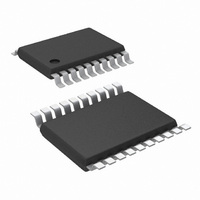
LM5118Q1MHX/NOPB National Semiconductor, LM5118Q1MHX/NOPB Datasheet

LM5118Q1MHX/NOPB
Specifications of LM5118Q1MHX/NOPB
Available stocks
Related parts for LM5118Q1MHX/NOPB
LM5118Q1MHX/NOPB Summary of contents
Page 1
... The device is available in a power enhanced TSSOP-20 package featuring an exposed die attach pad to aid thermal dissipation. Typical Application Circuit © 2011 National Semiconductor Corporation LM5118/LM5118Q Features ■ LM5118Q is an Automotive Grade product that is AEC- Q100 grade 1 qualified (-40° ...
Page 2
Connection Diagram Ordering Information Ordering Number Package Type LM5118MH TSSOP-20EP LM5118MHX TSSOP-20EP LM5118Q1MH TSSOP-20EP LM5118Q1MHX TSSOP-20EP *Automotive Grade (Q) product incorporates enhanced manufacturing and support processes for the automotive market, including defect detection methodologies. Reliability qualification is compliant with the ...
Page 3
Pin Name Description 11 SYNC Sync input for switching regulator synchronization to an external clock Current sense input. Connect to the diode side of the current sense resistor. 13 CSG Current sense ground input. Connect to the ground ...
Page 4
... Absolute Maximum Ratings If Military/Aerospace specified devices are required, please contact the National Semiconductor Sales Office/ Distributors for availability and specifications. VIN, EN, VOUT to GND VCC, LO, VCCX, UVLO to GND (Note GND CSG GND Electrical Characteristics junction temperature range of -40°C to +125°C. Unless otherwise specified, the following conditions apply: VIN = 48V, VCCX = 0V 5V 29.11 kΩ ...
Page 5
Symbol Parameter COMP Sink/Source Current A DC Gain OL f Unity Bain Bandwidth BW PWM COMPARATORS t Forced HO Off-time HO(OFF) T Minimum HO On-time ON(MIN) COMP to Comparator Offset OSCILLATOR (RT PIN) f Frequency 1 SW1 f Frequency 2 ...
Page 6
Note 1: Absolute Maximum Ratings are limits beyond which damage to the device may occur. Operating Ratings indicate conditions for which the device is intended to be functional, but does not guarantee specific performance limits. For guaranteed specifications and test ...
Page 7
Typical Performance Characteristics Efficiency vs VIN and IOUT VOUT = 12V VCC vs VIN Error Amplifier Gain/Phase Current Limit Threshold vs VOUT/VIN 30058503 30058505 LO and HO Peak Gate Current vs Output Voltage 30058507 7 VOUT = 12V 30058504 VCC ...
Page 8
Oscillator Frequency vs RT www.national.com 30058509 8 ...
Page 9
Block Diagram and Typical Application Circuit 9 www.national.com ...
Page 10
Detailed Operating Description The LM5118 high voltage switching regulator features all of the functions necessary to implement an efficient high voltage buck or buck-boost regulator using a minimum of external components. The regulator switches smoothly from buck to buck-boost operation ...
Page 11
FIGURE 4. Mode Dependence on Duty Cycle (VOUT =12V) Operation Modes Figure 4 illustrates how duty cycle affects the operational mode and is useful for reference in the following discussions. Initially, only the buck switch is active and the buck ...
Page 12
FIGURE 5. Buck (HO) and Boost (LO) Switch Duty Cycle vs. Time, Illustrating Gradual Mode Change with Decreasing Input Voltage High Voltage Start-Up Regulator The LM5118 contains a dual mode, high voltage linear regu- lator that provides the VCC bias ...
Page 13
The EN pin can be tied directly to the VIN pin if this function is not needed. It must not be left floating MΩ pull-up resistor to VIN can be used ...
Page 14
Error Amplifier and PWM Comparator The internal high gain error amplifier generates an error signal proportional to the difference between the regulated output voltage and an internal precision reference (1.23V). The out- put of the error amplifier is connected to ...
Page 15
Where g is the ramp generator transconductance (5 µA/V) m and A is the current sense amplifier gain (10V/V). The ramp capacitor should be located very close to the device and con- nected directly to the RAMP and AGND pins. ...
Page 16
Maximum Duty Cycle Each conduction cycle of the buck switch is followed by a forced minimum off-time of 400ns to allow sufficient time for the re-circulating diode current to be sampled. This forced off- time limits the maximum duty cycle ...
Page 17
FIGURE 12. Inductor Current Waveform INDUCTOR SELECTION L1 The inductor value is determined based upon the operating frequency, load current, ripple current and the input and out- put voltages. Refer to Figure 12 for details. To keep the circuit in ...
Page 18
Buck-boost mode capacitance can be estimated from: ESR requirements can be estimated from: For our example, with a ΔVOUT (output ripple mV 141 µF MIN ESR = 3.8 mΩ ...
Page 19
ICout For this application, a C16 value of 0.1 µF was chosen which corresponds to a soft-start time of about 12 ms. R8 and R9 set the output voltage level, the ratio ...
Page 20
RHP zero. The error amplifier zero (see below) should be placed near the dominate modulator pole. This is a good starting point for compensation. Refer to the on-line LM5118 Quick-Start calculator for ready to use ...
Page 21
The plots shown in Figures 13, 14 and 15 illustrate the gain and phase diagrams of the design example. The overall band- width is lower in a buck-boost application due the compen- sation challenges associated with the right-half-plane zero. For ...
Page 22
PCB Layout and Thermal Considerations In a buck-boost regulator, there are two loops where currents are switched very fast. The first loop starts from the input ca- pacitors, and then to the buck switch, the inductor, the boost switch then ...
Page 23
23 www.national.com ...
Page 24
Physical Dimensions www.national.com inches (millimeters) unless otherwise noted TSSOP-20EP Outline Drawing NS Package Number MXA20A 24 ...
Page 25
Notes 25 www.national.com ...
Page 26
... For more National Semiconductor product information and proven design tools, visit the following Web sites at: www.national.com Products Amplifiers www.national.com/amplifiers Audio www.national.com/audio Clock and Timing www.national.com/timing Data Converters www.national.com/adc Interface www.national.com/interface LVDS www.national.com/lvds Power Management www.national.com/power Switching Regulators www.national.com/switchers LDOs www.national.com/ldo LED Lighting www ...


