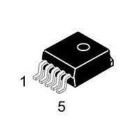
LM2596DSADJG ON Semiconductor, LM2596DSADJG Datasheet

LM2596DSADJG
Specifications of LM2596DSADJG
Available stocks
Related parts for LM2596DSADJG
LM2596DSADJG Summary of contents
Page 1
LM2596 3.0 A, Step-Down Switching Regulator The LM2596 regulator is monolithic integrated circuit ideally suited for easy and convenient design of a step−down switching regulator (buck converter capable of driving a 3.0 A load with excellent line and ...
Page 2
Typical Application (Adjustable Output Voltage Version Unregulated DC Input 100 mF +V Unregulated in DC Input Feedback R2 Fixed Gain C Error Amplifier 1.235 V Band-Gap Reference Figure 1. Typical Application and ...
Page 3
PIN FUNCTION DESCRIPTION Pin Symbol 1 V This pin is the positive input supply for the LM2596 step−down switching regulator. In order to minimize voltage transi- in ents and to supply the switching currents needed by the regulator, a suitable ...
Page 4
SYSTEM PARAMETERS ELECTRICAL CHARACTERISTICS over full Operating Temperature Range −40°C to +125°C Characteristics LM2596 (Note 1, Test Circuit Figure 15) Feedback Voltage ( 0 Load Feedback Voltage (8.5 V ≤ V ≤ ...
Page 5
TYPICAL PERFORMANCE CHARACTERISTICS 1 0 500 mA Load 0.6 Normalized 25°C J 0.4 0.2 0 -0.2 -0.4 -0.6 -0.8 -1.0 -50 - JUNCTION TEMPERATURE (°C) ...
Page 6
TYPICAL PERFORMANCE CHARACTERISTICS 200 180 160 T = 25°C 140 J 120 100 INPUT VOLTAGE (V) in Figure 8. Standby Quiescent Current 1.0 0 ...
Page 7
TYPICAL PERFORMANCE CHARACTERISTICS ms/div Figure 13. Switching Waveforms Vout = Output Pin Voltage, 10 V/div B: Switch Current, 2.0 ...
Page 8
As in any switching regulator, the layout of the printed circuit board is very important. Rapidly switching currents associated with wiring inductance, stray capacitance and parasitic inductance of the printed circuit board traces can generate voltage transients which electromagnetic interferences ...
Page 9
PROCEDURE (ADJUSTABLE OUTPUT VERSION: LM2596) Procedure Given Parameters Regulated Output Voltage out V = Maximum DC Input Voltage in(max Maximum Load Current Load(max) 1. Programming Output Voltage To select the right programming resistor R1 and R2 ...
Page 10
PROCEDURE (ADJUSTABLE OUTPUT VERSION: LM2596) (CONTINUED) Procedure 4. Inductor Selection (L1) A. Use the following formula to calculate the inductor Volt x microsecond [V x ms] constant: V OUT OUT SAT ...
Page 11
LM2596 Series Buck Regulator Design Procedures Table 1. RECOMMENDED VALUES OF THE OUTPUT CAPACITOR AND FEEDFORWARD CAPACITOR ( load V ( 1500/35/24 1000/35/29 26 1200/35/26 820/35 22 1000/35/29 680/35/36 20 820/35/32 470/35/46 18 820/35/32 470/35/46 ...
Page 12
... MBRS340T3 31DQ04 MBRD340 50 V MBR350 SK35 31DQ05 30WQ05 SR305 60 V MBR360 MBRS360T3 DQ06 MBRD360 SR306 NOTE: Diodes listed in bold are available from ON Semiconductor. 4.0 − 6.0 A Through Surface Through Hole Mount Hole 1N5823 SR502 SB520 1N5824 50WQ03 SR503 MUR320 SB530 31DF1 ...
Page 13
Table 3. INDUCTOR MANUFACTURERS PART NUMBERS Schott Through Inductance Current Hole (mH) (A) L15 22 0.99 67148350 L21 68 0.99 67144070 L22 47 1.17 67144080 L23 33 1.40 67144090 L24 22 1.70 67148370 L25 15 2.10 67148380 L26 330 0.80 ...
Page 14
EXTERNAL COMPONENTS Input Capacitor ( The Input Capacitor Should Have a Low ESR For stable operation of the switch mode converter a low ESR (Equivalent Series Resistance) aluminium or solid tantalum bypass capacitor is needed between the input ...
Page 15
Catch Diode Locate the Catch Diode Close to the LM2596 The LM2596 is a step−down buck converter; it requires a fast diode to provide a return path for the inductor current when the switch turns off. This diode must be ...
Page 16
A toroid, pot core or E−core (closed magnetic structure) should be used in such applications. Do Not Operate an Inductor Beyond its Maximum ...
Page 17
If improvements are needed, double sided or multilayer PC boards with large copper areas should be considered. In order to achieve the best thermal performance highly recommended to use wide copper traces as well as ...
Page 18
ADDITIONAL APPLICATIONS Inverting Regulator An inverting buck−boost regulator LM2596−ADJ is shown in Figure 22. This circuit converts a positive input voltage to a negative output voltage with a common ground by bootstrapping the regulators ground to the negative output voltage. ...
Page 19
100 Shutdown Input 5.0 V Off 470 MOC8101 NOTE: This picture does not show the complete circuit. Figure 24. Inverting Buck−Boost Regulator Shutdown Circuit Using an Optocoupler With ...
Page 20
Delayed Startup There are some applications, like the inverting regulator already mentioned above, which require a higher amount of startup current. In such cases, if the input power source is limited, this delayed startup feature becomes very useful. To provide ...
Page 21
V Max Unregulated DC Input +V in LM2596−Adj ON/OFF in 100 mF D Figure 30. 1 Adjustable 3.0 A Power Supply with Low Output Ripple Feedback Output ...
Page 22
THE LM2596 STEP−DOWN VOLTAGE REGULATOR WITH 5 3.0 A OUTPUT POWER CAPABILITY. TYPICAL APPLICATION WITH THROUGH−HOLE PC BOARD LAYOUT Unregulated +V DC Input in LM2596−ADJ ...
Page 23
... ORDERING INFORMATION Device LM2596TADJG LM2596TVADJG LM2596DSADJG LM2596DSADJR4G †For information on tape and reel specifications, including part orientation and tape sizes, please refer to our Tape and Reel Packaging Specifications Brochure, BRD8011/D. TO−220 TV SUFFIX CASE 314B LM 2596T−ADJ AWLYWWG 1 5 Package TO−220 (Pb−Free) TO−220 (F) (Pb− ...
Page 24
B −P− OPTIONAL Q CHAMFER 0.24 (0.610 0.10 (0.254 −Q− B1 DETAIL A 0.356 (0.014) T ...
Page 25
... Pb−Free strategy and soldering details, please download the ON Semiconductor Soldering and Mounting Techniques Reference Manual, SOLDERRM/D. ON Semiconductor and are registered trademarks of Semiconductor Components Industries, LLC (SCILLC). SCILLC reserves the right to make changes without further notice to any products herein ...


