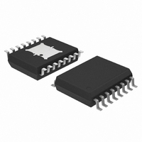
NCP3163PWG ON Semiconductor, NCP3163PWG Datasheet

NCP3163PWG
Specifications of NCP3163PWG
Available stocks
Related parts for NCP3163PWG
NCP3163PWG Summary of contents
Page 1
... ORDERING INFORMATION See detailed ordering and shipping information in the package dimensions section on page 18 of this data sheet. *For additional information on our Pb−Free strategy and soldering details, please download the ON Semiconductor Soldering and Mounting Techniques Reference Manual, SOLDERRM/D. Publication Order Number: NCP3163/D 18 ...
Page 2
I PKsense Timing Capacitor C T Shutdown R DT Gnd Voltage Feedback 1 Voltage Feedback 2 LVI Output PIN FUNCTION DESCRIPTION SOIC16 DFN18 PIN NAME 1 15 LVI Output 2 16 Voltage Feedback ...
Page 3
MAXIMUM RATINGS (Note 1) Rating Power Supply Voltage Switch Collector Voltage Range Switch Emitter Voltage Range Switch Collector to Emitter Voltage Switch Current Driver Collector Voltage (Pin 8) Driver Collector Current (Pin 8) Bootstrap Input Current Range Current Sense Input ...
Page 4
ELECTRICAL CHARACTERISTICS values T is the operating ambient temperature range that applies (Note 7), unless otherwise noted.) A Characteristic OSCILLATOR Frequency T = 25° Total Variation over ...
Page 5
T , AMBIENT TEMPERATURE (°C) A Figure 4. Oscillator Frequency Change vs. Temperature when only C is connected ...
Page 6
V CC Pin 2.4 2.0 1.6 1 AMBIENT TEMPERATURE (°C) A Figure 8. Bootstrap Input Current Source vs. Temperature 0 Darlington Configuration V CC Emitter Sourcing Current ...
Page 7
252 250 248 246 - AMBIENT TEMPERATURE (°C) A Figure 14. Current Limit Comparator Threshold Voltage vs. Temperature 8.0 6.0 4.0 Pins ...
Page 8
The NCP3163 is a monolithic power switching regulator optimized for DC−to−DC converter applications. The combination of its features enables the system designer to directly implement step−up, step−down, and voltage− inverting converters with a minimum number of external components. Potential applications ...
Page 9
Feedback and Low Voltage Indicator Comparators Output voltage control is established by the Feedback comparator. The inverting input is internally biased at 1.25 V and is not pinned out. The converter output voltage is typically divided down with two external ...
Page 10
When configured for step−down or voltage−inverting applications (see application notes at the end of this document) the inductor will forward bias the output rectifier when the switch turns off. Rectifiers with a high forward voltage drop or long turn−on delay ...
Page 11
Calculation Step−Down (See Notes 1,2,3) V out ) off sat * V out off ƒ off 32.143 · ...
Page 12
Figure 23. Typical Buck Application Schematic Value of Components Name Value ...
Page 13
Figure 24. Buck Layout APPLICATION SPECIFIC CHARACTERISTICS 85 5.0 V Eff 80 75 3.3 V Eff 0.5 1.0 1.5 I (A) out Figure 25. Efficiency vs. Output Current for the Buck Demo Board at ...
Page 14
Figure 26. Typical Boost Application Schematic Value of Components for out Name Value Schottky Rectifier C ...
Page 15
Figure 27. Boost Demo Board Layout 0.1 0.2 0.3 0.4 0.5 I (A) out Figure 28. Efficiency vs. Output Current for the Boost Demo Board http://onsemi.com ...
Page 16
Figure 29. Typical Voltage Inverting Application Schematic Value of Components for V = −15 V out Name Value Schottky Rectifier C 270 mF, 16 ...
Page 17
Figure 30. Voltage Inverting Demo Board Layout 0.1 0.15 0.2 0.25 0.3 0.35 I (A) out Figure 31. Efficiency vs. Output Current for the Voltage Inverting Demo Board http://onsemi.com 17 0.4 ...
Page 18
... ORDERING INFORMATION Device NCP3163PWG NCP3163PWR2G NCP3163BPWG NCP3163BPWR2G NCP3163MNR2G NCP3163BMNR2G NCV3163PWG NCV3163PWR2G NCV3163MNR2G †For information on tape and reel specifications, including part orientation and tape sizes, please refer to our Tape and Reel Packaging Specifications Brochure, BRD8011/D. Package SOIC−16 W Exposed Pad (Pb−Free) SOIC−16 W Exposed Pad (Pb− ...
Page 19
... L SOLDERING FOOTPRINT* 0.175 0.050 0.200 0.074 0.024 *For additional information on our Pb−Free strategy and soldering details, please download the ON Semiconductor Soldering and Mounting Techniques Reference Manual, SOLDERRM/D. http://onsemi.com 19 NOTES: 1. DIMENSIONING AND TOLERANCING PER ANSI Y14.5M, 1982. 2. CONTROLLING DIMENSION: MILLIMETER. 3. DIMENSION A AND B DO NOT INCLUDE MOLD PROTRUSION ...
Page 20
... A B 0.05 C NOTE 3 *For additional information on our Pb−Free strategy and soldering details, please download the ON Semiconductor Soldering and Mounting Techniques Reference Manual, SOLDERRM/D. N. American Technical Support: 800−282−9855 Toll Free USA/Canada Europe, Middle East and Africa Technical Support: Phone: 421 33 790 2910 Japan Customer Focus Center Phone: 81− ...


