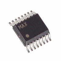
MAX15046BAEE+T Maxim Integrated Products, MAX15046BAEE+T Datasheet - Page 18

MAX15046BAEE+T
Manufacturer Part Number
MAX15046BAEE+T
Description
IC CTLR SYNC BUCK 40V 16-QSOP
Manufacturer
Maxim Integrated Products
Type
Step-Down (Buck)r
Datasheet
1.MAX15046BAEET.pdf
(24 pages)
Specifications of MAX15046BAEE+T
Internal Switch(s)
No
Synchronous Rectifier
Yes
Number Of Outputs
1
Voltage - Output
0.6 ~ 34 V
Current - Output
3A
Frequency - Switching
100kHz ~ 1MHz
Voltage - Input
4.5 ~ 40 V
Operating Temperature
-40°C ~ 125°C
Mounting Type
Surface Mount
Package / Case
16-QSOP
Power - Output
771.5mW
Lead Free Status / RoHS Status
Lead free / RoHS Compliant
40V, High-Performance, Synchronous
Buck Controller
So:
2) The gain of the modulator (GAIN
the pulse-width modulator, LC filter, feedback divider,
and associated circuitry at crossover frequency is:
The gain of the error amplifier (GAIN
frequencies is:
The total loop gain as the product of the modulator gain
and the error amplifier gain at f
3) Use the second pole (f
< f
does not flatten out soon after the 0dB crossover, and
maintains -20dB/decade slope up to 1/2 of the switching
frequency. This is likely to occur if the output capacitor
is low-ESR tantalum. Set f
When using a ceramic capacitor, the capacitor ESR
zero (f
of the switching frequency, f
this case, place the frequency of the second pole (f
high enough in order not to significantly erode the phase
margin at the crossover frequency. For example, set f
at 5 x f
crossover frequency f
18
So :
Solving for C :
V
RAMP
V
ZO
GAIN
IN
_____________________________________________________________________________________
< f
ZO
O
×
C
MOD
SW/2
) is likely to be located even above one half
(2
I
so that the contribution to phase loss at the
=
π ×
I
V
. The frequency response of the loop gain
=
RAMP
GAIN
f )
O
C
V
GAIN
RAMP
F
2
V
IN
=
×
EA
×
C
MOD
O
2
(
1
f
2
P2
π ×
OUT
= π ×
π ×
is only about 11N:
×
P2
V
2
P2
= 5 x f
(2
R
IN
×
f
) to cancel f
O
F
×
π ×
GAIN
= f
×
L
PO
×
×
f
1
R
O
OUT
0.8 f
O
L
ZO
f )
F
O
O
×
OUT
< f
is 1.
EA
.
C
×
2
× π ×
I
O
MOD
PO
×
×
=
2
×
L
R
< f
1
C
1
ZO
EA
OUT
F
OUT
), comprised of
SW/2
f
O
when f
) in midband
×
)
×
C
C
< f
I
OUT
×
PO
R
ZO
F
< f
. In
P2
=
P2
O
1
)
Once f
4) Place the second zero (f
whichever is lower and calculate R
equation:
5) Place the third pole (f
frequency and calculate C
6) Calculate R
The MAX15046 step-down controller drives two exter-
nal logic-level n-channel MOSFETs. The key selection
parameters to choose these MOSFETs include:
U On-resistance (R
U Maximum Drain-to-Source Voltage (V
U Minimum Threshold Voltage (V
U Total Gate Charge (Q
U Reverse Transfer Capacitance (C
U Power Dissipation
The two n-channel MOSFETs must be a logic-level
type with guaranteed on-resistance specifications at
V
side MOSFET that has conduction losses equal to the
switching losses at the typical input voltage. Ensure that
the conduction losses at minimum input voltage do not
exceed the MOSFET package thermal limits, or violate
the overall thermal budget. Also ensure that the conduc-
tion losses plus switching losses at the maximum input
voltage do not exceed package ratings or violate the
GS
= 4.5V. For maximum efficiency, choose a high-
P2
is known, calculate R
C
CF
2
as:
=
R
R
(
DS(ON)
2
2
1
R
π ×
=
=
I
=
2
V
0.5 f
G
π ×
OUT
2
)
π ×
)
P3
CF
×
V
f
Z2
1
FB
) at one half the switching
SW
f
−
:
P2
Z2
1
C
×
V
I
:
F
) at 0.2 x f
C
FB
×
×
TH(MIN)
MOSFET Selection
I
R
C
- R
×
F
RSS
1
I
R
×
using the following
I
1
C
DS(MAX)
)
)
F
)
- 1
O
or at f
)
PO
,


