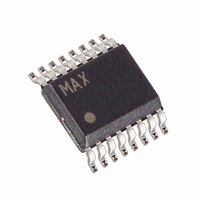
MAX15046BAEE+ Maxim Integrated Products, MAX15046BAEE+ Datasheet - Page 8

MAX15046BAEE+
Manufacturer Part Number
MAX15046BAEE+
Description
IC CTLR SYNC BUCK 40V 16-QSOP
Manufacturer
Maxim Integrated Products
Type
Step-Down (Buck)r
Datasheet
1.MAX15046BAEET.pdf
(24 pages)
Specifications of MAX15046BAEE+
Internal Switch(s)
No
Synchronous Rectifier
Yes
Number Of Outputs
1
Voltage - Output
0.6 ~ 34 V
Current - Output
3A
Frequency - Switching
100kHz ~ 1MHz
Voltage - Input
4.5 ~ 40 V
Operating Temperature
-40°C ~ 125°C
Mounting Type
Surface Mount
Package / Case
16-QSOP
Power - Output
771.5mW
Output Voltage
0.6 V to 34 V
Output Current
25 A
Output Power
1818.2 mW
Input Voltage
4.5 V to 40 V
Switching Frequency
100 KHz to 1000 KHz
Mounting Style
SMD/SMT
Duty Cycle (max)
87.5 %
Primary Input Voltage
40V
No. Of Outputs
1
No. Of Pins
16
Operating Temperature Range
-40°C To +125°C
Peak Reflow Compatible (260 C)
Yes
Rohs Compliant
Yes
Lead Free Status / RoHS Status
Lead free / RoHS Compliant
40V, High-Performance, Synchronous
Buck Controller
8
______________________________________________________________________________________
PIN
10
11
12
13
14
15
16
—
1
2
3
4
5
6
7
8
9
PGOOD
NAME
COMP
PGND
GND
DRV
V
BST
CSP
LIM
DH
EN
DL
FB
RT
LX
EP
IN
CC
Regulator Input. Connect to the input rail of the buck converter. Bypass IN to PGND with a 100nF
minimum ceramic capacitor. When operating in the 5V Q10% range, connect IN to V
5.25V Linear Regulator Output. Bypass V
when V
DRV.
Open-Drain Power-Good Output. Pull up PGOOD to an external power supply or output with an
external resistor.
Active-High Enable Input. Pull EN to GND to disable the buck converter output. Connect to V
for always-on operation. EN can be used for power sequencing and as a UVLO adjustment input.
Current-Limit Input. Connect a resistor from LIM to GND to program the current-limit threshold from
30mV (R
Error-Amplifier Output. Connect compensation network from COMP to FB or from COMP to GND.
Feedback Input (Inverting Input of Error Amplifier). Connect FB to a resistive divider between the
buck converter output and GND to adjust the output voltage from 0.6V up to 0.85 x IN.
Oscillator-Timing Resistor Input. Connect a resistor from RT to GND to set the oscillator frequency
from 100kHz to 1MHz.
Analog Ground. Connect PGND and AGND together at a single point.
Power Ground. Use PGND as a return path for the low-side MOSFET gate driver.
Gate-Driver Supply Voltage. DRV is internally connected to the low-side driver supply. Bypass DRV to
PGND with a 2.2FF minimum ceramic capacitor (see the Typical Application Circuits).
Low-Side External MOSFET Gate-Driver Output. DL swings from DRV to PGND.
Boost Flying Capacitor Connection. Internally connected to the high-side driver supply. Connect a
ceramic capacitor of at least 100nF between BST and LX and a diode between BST and DRV for
the high-side MOSFET gate-driver supply.
Inductor Connection. Also serves as a return terminal for the high-side MOSFET driver current.
Connect LX to the switching side of the inductor.
High-Side External MOSFET Gate-Driver Output. DH swings from BST to LX.
Current-Sense Positive Input. Connect to the drain of low-side MOSFET with Kelvin connection.
Exposed Pad. EP is internally connected to ground. Connect EP to a large copper ground plane to
maximize thermal performance.
CC
LIM
supplies MOSFET gate-driver current at DRV or 2.2FF when V
= 6kI) to 300mV (R
LIM
= 60kI).
CC
FUNCTION
to PGND with a ceramic capacitor of at least 4.7FF
Pin Description
CC
is not used to power
CC
.
CC


