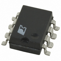
TOP414G Power Integrations, TOP414G Datasheet - Page 3

TOP414G
Manufacturer Part Number
TOP414G
Description
IC SW PWM DC-DC 48VDC 12W 8SMD
Manufacturer
Power Integrations
Series
TOPSwitch®r
Type
Step-Down (Buck), Step-Up (Boost), Flyback, Forward Converterr
Datasheet
1.TOP414GN-TL.pdf
(16 pages)
Specifications of TOP414G
Internal Switch(s)
Yes
Synchronous Rectifier
No
Number Of Outputs
1
Frequency - Switching
120kHz
Operating Temperature
-40°C ~ 125°C
Mounting Type
Surface Mount
Package / Case
8-SMD Gull Wing
Output Voltage
5.8 V
Input / Supply Voltage (max)
265 VAC
Input / Supply Voltage (min)
85 VAC
Duty Cycle (max)
70 %
Switching Frequency
120 KHz
Supply Current
1.4 mA
Operating Temperature Range
- 40 C to + 150 C
Mounting Style
SMD/SMT
Lead Free Status / RoHS Status
Contains lead / RoHS non-compliant
Current - Output
-
Voltage - Output
-
Voltage - Input
-
Power - Output
-
Lead Free Status / Rohs Status
Lead free / RoHS Compliant
Available stocks
Company
Part Number
Manufacturer
Quantity
Price
Part Number:
TOP414G
Manufacturer:
POWER
Quantity:
20 000
Company:
Part Number:
TOP414GN
Manufacturer:
INFINEON
Quantity:
164
Company:
Part Number:
TOP414GN
Manufacturer:
PowerInt
Quantity:
50
Part Number:
TOP414GN
Manufacturer:
POWER
Quantity:
20 000
Company:
Part Number:
TOP414GN-TL
Manufacturer:
POWER
Quantity:
12 000
Part Number:
TOP414GN-TL
Manufacturer:
POWER
Quantity:
20 000
TOPSwitch Family Functional Description
TOPSwitch is a self biased and protected linear control current-
to-duty cycle converter with an open drain output. High
efficiency is achieved through the use of CMOS and integration
of the maximum number of functions possible. CMOS
significantly reduces bias currents as compared to bipolar or
discrete solutions. Integration eliminates external power resistors
used for current sensing and/or supplying initial start-up bias
current.
During normal operation, the internal output MOSFET duty
cycle linearly decreases with increasing CONTROL pin current
as shown in Figure 4. To implement all the required control,
bias, and protection functions, the DRAIN and CONTROL pins
each perform several functions as described below. Refer to
Figure 2 for a block diagram and Figure 6 for timing and voltage
waveforms of the TOPSwitch integrated circuit.
Control Voltage Supply
CONTROL pin voltage V
controller and driver circuitry. An external bypass capacitor
closely connected between the CONTROL and SOURCE pins
is required to supply the gate drive current. The total amount of
capacitance connected to this pin (C
timing as well as control loop compensation. V
either of two modes of operation. Hysteretic regulation is used
for initial start-up and overload operation. Shunt regulation is
used to separate the duty cycle error signal from the control
circuit supply current. During start-up, V
from a high-voltage switched current source connected internally
between the DRAIN and CONTROL pins. The current source
provides sufficient current to supply the control circuitry as
well as charge the total external capacitance (C
C
is the supply or bias voltage for the
T
) also sets the auto-restart
C
current is supplied
C
T
is regulated in
).
Figure 4. Relationship of Duty Cycle to CONTROL Pin Current.
Figure 5. Start-up Waveforms for (a) Normal Operation and (b)
DRAIN
DRAIN
V C
V C
D MAX
D MIN
5.7 V
4.7 V
5.7 V
4.7 V
V IN
V IN
Auto-restart
Auto-restart.
0
0
0
0
I CD1
Charging C T
Charging C T
C
T
connected to the CONTROL pin
Off
Off
I C
I C
is the total external capacitance
2.5
Switching
I B
(a)
(b)
Discharging C T
I C (mA)
Slope = PWM Gain
Off
I CD1
95%
8 Cycles
TOP412/414
Switching
-16%/mA
6.5
Switching
5%
Discharging C T
4/99
I CD2
PI-1124A-060694
Off
A
PI-1691-112895
45
3


