ADMC200AP Analog Devices Inc, ADMC200AP Datasheet
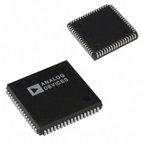
IC MOTION CO-PROC 12.5MHZ 68PLCC

ADMC200AP

Manufacturer Part Number
ADMC200AP
Description
IC MOTION CO-PROC 12.5MHZ 68PLCC
Manufacturer
Analog Devices Inc
Datasheet

Specifications of ADMC200AP

Rohs Status
RoHS non-compliant
Applications
*
Mounting Type
Surface Mount
Package / Case
68-PLCC
a
REV. B
GENERAL DESCRIPTION
The ADMC200 is a motion coprocessor that can be used with
either microcontrollers or digital signal processors (DSP). It
provides the functionality that is required to implement a digital
control system. In a typical application, the DSP or micro-
controller performs the control algorithms (position, speed,
torque and flux loops) and the ADMC200 provides the neces-
sary motor control functions: analog current data acquisition,
vector transformation, and PWM drive signals.
PRODUCT HIGHLIGHTS
Simultaneous Sampling of Four Inputs
A four channel sample and hold amplifier allows three-phase
motor currents to be sampled simultaneously, reducing errors
from phase coherency. Sample and hold acquisition time is
1.6 s and conversion time per channel is 3.2 s (using a 12.5 MHz
system clock).
Information furnished by Analog Devices is believed to be accurate and
reliable. However, no responsibility is assumed by Analog Devices for its
use, nor for any infringements of patents or other rights of third parties
which may result from its use. No license is granted by implication or
otherwise under any patent or patent rights of Analog Devices.
FEATURES
Analog Input Block
12-Bit PWM Timer Block
Vector Transformation Block
DSP & Microcontroller Interface
6.25 MHz to 25 MHz Operating Clock Range
68-Lead PLCC Package
Single 5 V DC Power Supply
Industrial Temperature Range
11-Bit Resolution Analog-to-Digital (A/D) Converter
4 Single-Ended Simultaneously Sampled Analog Inputs
3.2 s Conversion Time/Channel
0 V–5 V Analog Input Range
Internal 2.5 V Reference
PWM Synchronized Sampling Capability
Three-Phase Center-Based PWM
1.5 kHz–25 kHz PWM Switching Frequency Range
Programmable Deadtime
Programmable Pulse Deletion
PWM Synchronized Output
External PWM Shutdown
12-Bit Vector Transformations
Forward and Reverse Clarke Transformations
Forward and Reverse Park Rotations
2.9 s Transformation Time
12-Bit Memory Mapped Registers
Twos Complement Data Format
Flexible Analog Channel Sequencing
The ADMC200 support acquisition of 2, 3, or 4 channels per
group. Converted channel results are stored in registers and the
data can be read in any order. The sampling and conversion
time for two channels is 8 s, three channels is 11.2 s, and four
channels is 14.4 s (using a 12.5 MHz system clock).
Embedded Control Sequencer
The embedded control sequencer off-loads the DSP or micro-
processor, reducing the instructions required to read analog in-
put channels, control PWM timers and perform vector trans-
formations. This frees the host processor for performing control
algorithms.
Fast DSP/Microprocessor Interface
The high speed digital interface allows direct connection to
16-bit digital signal processors and microprocessors. The
ADMC200 has 12 bit memory mapped registers with twos
complement data format and can be mapped directly into the
data memory map of a DSP. This allows for a single instruction
read and write interface.
Integration
The ADMC200 integrates a four channel simultaneous sam-
pling analog-to-digital converter, analog reference, vector trans-
formation, and three-phase PWM timers into a 68-lead PLCC.
Integration reduces cost, board space, power consumption, and
design and test time.
One Technology Way, P.O. Box 9106, Norwood, MA 02062-9106, U.S.A.
Tel: 781/329-4700
Fax: 781/326-8703
PWMSYNC
REFOUT
CONVST
RESET
REFIN
STOP
A0–3
AUX
CLK
IRQ
WR
RD
CS
AP
BP
CP
W
U
V
A
B
C
FUNCTIONAL BLOCK DIAGRAM
CONVERTER
SEQUENCER
REFERENCE
EMBEDDED
PWM TIMER
INTERNAL
CONTROL
11-BIT
BLOCK
12-BIT
A/D
World Wide Web Site: http://www.analog.com
Motion Coprocessor
D0 – D11
© Analog Devices, Inc., 2000
ADMC200
CONTROL BUS
TRANSFORMATION
REGISTERS
DATABUS
CONTROL
VECTOR
BLOCK

Related parts for ADMC200AP

ADMC200AP Summary of contents

Page 1

FEATURES Analog Input Block 11-Bit Resolution Analog-to-Digital (A/D) Converter 4 Single-Ended Simultaneously Sampled Analog Inputs 3.2 s Conversion Time/Channel 0 V–5 V Analog Input Range Internal 2.5 V Reference PWM Synchronized Sampling Capability 12-Bit PWM Timer Block Three-Phase Center-Based ...

Page 2

... Measurements made with external reference. 2 Tested with PWM Switching Frequency of 25 kHz. Specifications subject to change without notice 5%; AGND = DGND = 0 V; REFIN = 2.5 V; External Clock = DD 12.5 MHz – +85 C unless otherwise noted) A ADMC200AP Units 1 11 Bits 2 LSB max 2 LSB max 5 LSB max 4 ...

Page 3

Table I. Timing Specifications (V Number Symbol 1 t clk per 2 t clk pwh 3 t clk pwl 4 t csb_wrb addr_wrb data_wrb wrb_data wrb_addr hd 9 ...

Page 4

... Therefore, proper ESD precautions are recommended to avoid performance degradation or loss of functionality Figure 4. Read Cycle Timing Diagram Part DD Number DD DD ADMC200AP DD DD –4– ORDERING GUIDE Temperature Package Package Range Description Option – +85 C 68-Lead PLCC P-68A WARNING! ESD SENSITIVE DEVICE REV. B ...

Page 5

Pin Mnemonic Type Description 1 D9 BIDIR Data Bit 9 2 D10 BIDIR Data Bit 10 3 D11 BIDIR Data Bit 11, MSB 4– Connect 10 V SUP +5 V Digital Power Supply I/P Address ...

Page 6

ADMC200 ANALOG INPUT BLOCK The ADMC200 contains an 11-bit resolution, successive approxi- mation analog-to-digital (A/D) converter with twos complement output data format. The analog input range is 2 V–5 V) with a 2.5 V offset as defined by ...

Page 7

PWMTM register value. Note: Desired Pulse Density = (PWMCHx register)/( PWMTM register). The beginning of each PWM cycle is marked by the PWMSYNC signal. New values of ...

Page 8

ADMC200 Stationary Reference Frame Reference Frame Figure 9. Forward Park Transformation 120 V x Equivalent Three-Phase Stator Two-Phase Voltage Figure 10. Forward Clarke Transformation Operating/Using the Vector Transformation Block After powering up the ...

Page 9

When an interrupt occurs, the user must check Bit 1 of the system status register, SYSSTAT, to determine if the vector transformation block was the source of the interrupt. During the vector transformation, the transformation registers must not be ...

Page 10

ADMC200 ADDRESS BUS A0–A13 ADDRESS DECODE ADSP-2101/ DMS EN ADSP-2105/ ADSP-2115–20MHz IRQ2 ADSP-2171–10MHz RD ADSP-2181–10MHz WR CLKOUT D0–D23 DATA BUS *NOTE: BY MAPPING THE ADMC200 DATA BUS TO THE TWELVE HIGHEST BITS OF THE ADSP DATA BUS, FULL-SCALE OUTPUTS FROM ...

Page 11

Name ID/PHV1/VX IQ/PHV2 IX/PHV3 IY/VY ADCV ADCW ADCAUX ADCU SYSCTRL SYSSTAT DESCRIPTION OF THE REGISTERS All unspecified register locations are reserved. SYSCTRL System Control Register (See Table V and VI) SYSSTAT System Status Register (See Table VII) ADCU These registers ...

Page 12

ADMC200 IRQ Pin Format—Edge or Level Interrupt Selection. Bit 8 If Bit 8 is set to 0, then an interrupt will cause a pulse of one system clock to be generated on the IRQ pin. If Bit 8 is set ...

Related keywords