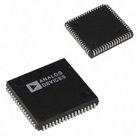
ADMC201AP Analog Devices Inc, ADMC201AP Datasheet - Page 11

ADMC201AP
Manufacturer Part Number
ADMC201AP
Description
IC MOTION CO-PROC 25MHZ 68PLCC
Manufacturer
Analog Devices Inc
Datasheet
1.ADMC201AP.pdf
(15 pages)
Specifications of ADMC201AP
Rohs Status
RoHS non-compliant
Applications
*
Mounting Type
Surface Mount
Package / Case
68-PLCC
Operating Temperature (min)
-40C
Operating Temperature (max)
85C
Operating Temperature Classification
Industrial
Mounting
Surface Mount
Lead Free Status / RoHS Status
Not Compliant
Available stocks
Company
Part Number
Manufacturer
Quantity
Price
Figure 12. TI Second Generation Devices TMS320C20/
C25/C25–50
In the case of the ADSP-2171/2181, the system clock is inter-
nally scaled, a 10 MHz system clock will derive a 20 MHz
CLKOUT. In the case of the TMS320C2X, the CLKOUT1
signal is derived from the system clock divided by a factor of 4,
consequently a 50 MHz TMS320C25-50 will derive a
12.5 MHz CLKOUT1 for use by the ADMC201.
Note: a pull-up resistor is required on the IRQ (Pin 18) output
from the ADMC201. The STOP (Pin 47) must be tied low if
not in use.
REV. B
DESCRIPTION OF THE REGISTERS
All unspecified register locations are reserved.
SYSCTRL
SYSSTAT
ADCU
ADCV
ADCW
ADCAUX
PWMTM
PWMCHA
PWMCHB
PWMCHC
PWMDT
PWMPD
ID/IQ
PHV1/2/3
TMS320C20
TMS320C25
TMS320C25-50
A0–A15
D0–D15
CLKOUT1
STRB
System Control Register (See Tables V,
VI, VII).
System Status Register (See Table VII).
These registers contain the results from
the first three analog input channels
U, V, and W. The output data format
is twos complement and, therefore, Bit 0
is always zero as the A/D converter
has 11-bit resolution.
This register contains the conversion result
of the auxiliary channels AUX0, AUX1,
AUX2 or AUX3.
PWM Master Switching Period
PWM Channel A On-Time
PWM Channel B On-Time
PWM Channel C On-Time
PWM Programmable Deadtime Value
PWM Programmable Pulse Deletion Value
These are the results of the reverse
rotation (torque and flux components).
These are the results from the forward
Clarke Transformation.
INTn
R/W
IS
ADDRESS BUS
DATA BUS
EN
ADDRESS
DECODE
V
DD
RD
CS
IRQ
WR
CLK
D0–D11
ADMC201
A0–A3
–11–
REGISTER ADDRESSING
Four address lines (A0 through A3) are used in conjunction
with the control lines (CS, WR, RD,) to select registers 0
through 15. The CS and RD control lines are active low. The
registers are given symbolic names.
PHIP1/2/3
IX/IY
VX, VY
RHOP
RHO
PIODATA
PIOCTRL
Pin
CS
RD
WR
Function
Enables the ADMC201 register interface
(connect via chip select logic-active low)
Places data from the internal register onto the
data bus
Loads the internal register with data on the
data bus on its positive edge
The inputs for reverse vector transforma-
tion (Clarke and Park).
These registers contain the results
of the Clarke transformation that
are the inputs to the reverse Park rotation.
VX, VY contain the results of the forward
Park rotation.
RHOP is the angle used during the
forward vector transformation. Writing to
the RHOP register causes the forward
rotation to start based on values in
RHOP, VD and VQ registers.
RHO is the angle used during the reverse
vector transformation. Writing to this
register starts the reverse rotation using
the values in the RHO, PHIP1/2/3
registers.
RHO and RHOP are unsigned ratios of
360 . For example, 45 degrees would be
45/360
Write to this register to change the
digital outputs and read from it to
determine the state of digital inputs.
This register is used to configure the
digital I/O as input or output and to
enable interrupt on change of state.
Table II.
2
12
.
ADMC201


