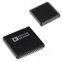
ADMC201AP Analog Devices Inc, ADMC201AP Datasheet - Page 6

ADMC201AP
Manufacturer Part Number
ADMC201AP
Description
IC MOTION CO-PROC 25MHZ 68PLCC
Manufacturer
Analog Devices Inc
Datasheet
1.ADMC201AP.pdf
(15 pages)
Specifications of ADMC201AP
Rohs Status
RoHS non-compliant
Applications
*
Mounting Type
Surface Mount
Package / Case
68-PLCC
Operating Temperature (min)
-40C
Operating Temperature (max)
85C
Operating Temperature Classification
Industrial
Mounting
Surface Mount
Lead Free Status / RoHS Status
Not Compliant
Available stocks
Company
Part Number
Manufacturer
Quantity
Price
ADMC201
ANALOG INPUT BLOCK
The ADMC201 contains an 11-bit resolution, successive approxi-
mation analog-to-digital (A/D) converter with twos complement
output data format. The analog input range is 2.5 V (0 V–5 V)
with a 2.5 V offset as defined by REFIN. The on-chip 2.5 V
5% reference is utilized by connecting the REFOUT pin to the
REFIN pin.
The input stage to the A/D converter is a four channel SHA
which allows the four channels (U, V, W and AUX) to be held
simultaneously and then sequentially digitized. The auxiliary
input (AUX) is fed by a four channel multiplexer that allows the
channels AUX0, AUX1, AUX2 and AUX3 to be individually
converted along with the primary channels U, V and W. The
auxiliary inputs are ideal for reading slower changing variables
such as bus voltage and temperature. The A/D conversion time
is determined by the system clock frequency, which can range
from 6.25 MHz to 12.5 MHz. The Sample and Hold (SHA)
acquisition time is 20 system clock cycles and is independent of
the number of channels sampled and/or digitized. Forty system
clock cycles are required to complete each A/D conversion. The
analog channel sampling is flexible and is programmable
through the SYSCTRL register. The minimum number of
channels per conversion is two. The throughput time of the
analog acquisition block can be calculated as follows:
where
A/D Conversions are initiated via the CONVST pin. A syn-
chronizing pulse (PWMSYNC) is provided at the beginning of
each PWM cycle. This pulse can be used to synchronize the
A/D conversion process to the PWM switching frequency.
Operating the A/D Converter
The A/D converter can be set up to convert a sequence of channels
as defined in the SYSCTRL register (see Table VI). The default
channel select mode after RESET is to convert channels V and
W only. This is two-/three-phase mode. Three-/three-phase
mode converts channels U, V, W, and/or AUX. Three-/three-
phase mode is selected by writing a 1 to Bit 3 of the SYSCTRL
register. After the conversion process is complete, the channels
can be read in any order.
There are two methods that can be used to indicate when the
A/D conversions are completed and the data is ready: interrupt
driven and software timing.
t
n = # channels,
t
t
AA
SHA
CONV
= analog acquisition time,
= SHA acquisition time (20 system clock period),
= conversion time (40 system clock period) per channel.
t
AA
t
SHA
(n t
CONV
)
–6–
Interrupt Driven Method
Interrupts can be used to indicate the end of conversion for a
group of channels. Before beginning any A/D conversions, Bit 7
of the SYSCTRL register must be set to 1 to enable A/D con-
version interrupts. Then, when an A/D conversion is complete,
an interrupt will be generated. After an interrupt is detected,
Bit 0 of the SYSSTAT register must be checked to determine if
the A/D converter was the source. Reading the SYSSTAT reg-
ister automatically clears the interrupt flag bits.
Software Timing Method
An alternative method is to use the DSP or microcontroller to
keep track of the amount of time elapsed between CONVST
and the expected completion time (n t
Reading Results
The 11-bit A/D conversion results for channels U, V, W and
AUX are stored in the ADCU, ADCV, ADCW and ADCAUX
registers respectively. The twos complement data is left justified
and the LSB is set to zero. The relationship between input volt-
age and output coding is shown in Figure 5.
Sample and Hold
After powering up the ADMC201, bring the RESET pin low for
a minimum of two clock cycles in order to enable A/D conversions.
Before initiating the first conversion (CONVST) after a reset,
the SHA time of 20 system clock cycles must occur. A conversion
is initiated by bringing CONVST high for a minimum of one
system clock cycle. The SHA goes into hold mode at the falling
edge of clock.
Following completion of the A/D conversion process, a minimum
of 20 system clock cycles are required before initiating another
conversion in order to allow the sample and hold circuitry to
reacquire the input signals.
If a CONVST is initiated before the 20 clock cycles have elapsed,
the embedded control sequencer will delay conversion until this
requirement is met.
0 0 0 0 0 0 0 0 0 0 0 0
1 0 0 0 0 0 0 0 0 0 0 0
0 1 1 1 1 1 1 1 1 1 1 0
Figure 5. Transfer Function
OUTPUT
CODE
0V
INPUT VOLTAGE
2.5
FULL-SCALE
TRANSITION
CONV
FS = 5V
LSB =
5V–1LSB
).
2048
5V
REV. B


