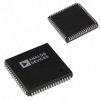
ADMC201AP Analog Devices Inc, ADMC201AP Datasheet - Page 7

ADMC201AP
Manufacturer Part Number
ADMC201AP
Description
IC MOTION CO-PROC 25MHZ 68PLCC
Manufacturer
Analog Devices Inc
Datasheet
1.ADMC201AP.pdf
(15 pages)
Specifications of ADMC201AP
Rohs Status
RoHS non-compliant
Applications
*
Mounting Type
Surface Mount
Package / Case
68-PLCC
Operating Temperature (min)
-40C
Operating Temperature (max)
85C
Operating Temperature Classification
Industrial
Mounting
Surface Mount
Lead Free Status / RoHS Status
Not Compliant
Available stocks
Company
Part Number
Manufacturer
Quantity
Price
REV. B
PWM TIMER BLOCK OVERVIEW
The PWM timers have 12-bit resolution and support program-
mable pulse deletion and deadtime. The ADMC201 generates
three center-based signals A, B and C based upon user-supplied
duty cycles values. The three signals are then complemented
and adjusted for programmable deadtime to produce the six
outputs. The ADMC201 PWM master switching frequency can
range from 2.5 kHz to 20 kHz, when using a 10 MHz system
clock. The master frequency selection is set as a fraction of the
PWMTM register. If the system clock is 10 MHz, then the
minimum edge resolution available is 100 ns.
The output format of the PWM block is active LO. There is an
external input to the PWM timers (STOP) that will disable all
six outputs within one system clock when the input is HIGH.
The ADMC201 has a PWM Synchronization output
(PWMSYNC) which brings out the master switching frequency
from the PWM timers. The width of the PWMSYNC pulse is
equal to one system clock cycle. For example, if the system clock
is 10 MHz, the PWMSYNC width would be equal to 100 ns.
PWM Master Switching Period Selection
The switching time is set by the PWMTM register which should
be loaded with a value equal to the system clock frequency
divided by the desired master switching frequency. For ex-
ample, if the desired switching frequency is 8 kHz and the
system clock frequency is 10 MHz, then the PWMTM register
should be loaded with 1250 (10 MHz/8 kHz). The PWMCHA,
PWMCHB and PWMCHC registers are loaded with the
desired on-time and their values would be calculated as a ratio
of the PWMTM register value. Note: Desired Pulse Density =
(PWMCHx register)/( PWMTM register).
The beginning of each PWM cycle is marked by the PWMSYNC
signal. New values of PWMCHA, PWMCHB and PWMCHC
must all be loaded into their respective registers at least four sys-
tem clock cycles before the beginning of a new PWM cycle. All
three registers must be updated for any of them to take effect.
New PWM on/off times are calculated during these four clock
cycles and therefore the PWMCHA, PWMCHB and PWMCHC
registers must be loaded before this time. If this timing require-
ment is not met, then the PWM outputs may be invalid during
the next PWM cycle.
PWM Example
The following example uses a system clock speed of 10 MHz.
The desired PWM master switching frequency is 8 kHz and the
desired on-time for the timers A, B and C are 25%, 50% and
10% respectively. The values for the PWMCHA, PWMCHB
and PWMCHC registers must be calculated as ratios of the
PWMTM register (1250 in this example). To achieve these
duty cycles, load the PWMCHA register with 313 (1250
0.25), PWMCHB with 625 (1250 0.5) and PWMCHC with
125 (1250
0.1).
–7–
Programmable Deadtime
With perfectly complemented PWM drive signals and nonideal
switching characteristics of the power devices, both transistors
in a particular leg might be switched on at the same time, result-
ing in either a power supply trip, inverter trip or device
destruction. In order to prevent this, a delay must be intro-
duced between the complemented signal edges. For example,
the rising edge of AP occurs before the falling edge of A, and the
falling edge of the complemented A occurs after the rising edge
of A. This capability is known as programmable deadtime.
The ADMC201 programmable deadtime value is loaded into
the 7-bit PWMDT register, in which the LSB is set to zero in-
ternally, which means the deadtime value is always divisible by
two. With a 10 MHz system clock, the 0–126 range of values in
PWMDT yield a range of deadtime values from 0 s to 12.6 s
in 200 ns steps. Figure 6 shows PWM timer A with a program-
mable deadtime of PWMDT.
Pulse Deletion
The pulse deletion feature prevents a pulse from being gener-
ated when the user-specified duty cycle results in a pulse
duration shorter than the user-specified deletion value. The
pulse deletion value is loaded into the 7-bit register PWMPD.
When the user-specified on-time for a channel would result in a
calculated pulse width less than the value specified in the
PWMPD register, then the PWM outputs for that channel
would be set to full off (0%) and its prime to full on (100%).
This is valid for A, AP, B, BP, C and CP. This feature would
be used in an environment where the inverter’s power transis-
tors have a minimum switching time. If the user-specified duty
cycle would result in a pulse duration shorter than the minimum
switching time of the transistors, then pulse deletion should be
used to prevent this occurrence. With a 10 MHz system clock,
the 0–127 range of values in PWMPD yield a range of deadtime
values from 0 s to 12.7 s in 100 ns steps.
External PWM Shutdown
There is an external input pin (STOP) to the PWM timers that
will disable all six outputs when it goes HIGH. When the STOP
pin goes HIGH, the PWM timer outputs will all go HIGH
within one system clock cycle. When the STOP pin goes LOW,
the PWM timer outputs are re-enabled within one system clock
cycle. If external PWM shutdown isn't required, tie the STOP
pin LOW.
Figure 6. Programmable Deadtime Example
AP
A
PWMCHA + PWMDT
PWMCHA - PWMDT
PWMTM
ADMC201


