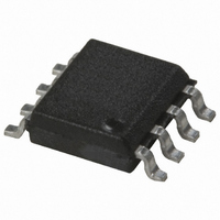
HCPL-0900 Avago Technologies US Inc., HCPL-0900 Datasheet - Page 11

HCPL-0900
Manufacturer Part Number
HCPL-0900
Description
ISOLATOR DIG 100MBD 1CH 8-SOIC
Manufacturer
Avago Technologies US Inc.
Datasheet
1.HCPL-0900-000E.pdf
(14 pages)
Specifications of HCPL-0900
Propagation Delay
12ns
Inputs - Side 1/side 2
1/0
Number Of Channels
1
Isolation Rating
2500Vrms
Voltage - Supply
3 V ~ 5.5 V
Data Rate
100MBd
Output Type
Tri-State
Package / Case
8-SOIC (3.9mm Width)
Operating Temperature
-40°C ~ 100°C
No. Of Channels
1
Isolation Voltage
2.5kV
Optocoupler Output Type
Logic Gate
Input Current
10µA
Output Voltage
5V
Opto Case Style
SOIC
No. Of Pins
8
Mounting Type
Surface Mount
Lead Free Status / RoHS Status
Contains lead / RoHS non-compliant
Other names
516-1150-5
Available stocks
Company
Part Number
Manufacturer
Quantity
Price
Part Number:
HCPL-0900
Manufacturer:
AGILENT
Quantity:
20 000
Part Number:
HCPL-0900-000E
Manufacturer:
AVAGO/安华高
Quantity:
20 000
Part Number:
HCPL-0900-000E/HCPL0900
Manufacturer:
AVAGO/安华高
Quantity:
20 000
Mixed 5V/3.3V or 3.3V/5V operation: Electrical Specifications
Test conditions that are not specified can be anywhere within the recommended operating range.
All typical specifications are at T
Parameter
HCPL-9000/-0900
HCPL-9030/-0930
HCPL-9031/-0931
HCPL-900J/-090J
HCPL-901J/-091J
HCPL-902J/-092J
Quiescent Supply Current 2
HCPL-9000/-0900
HCPL-9030/-0930
HCPL-9031/-0931
HCPL-900J/-090J
HCPL-901J/-091J
HCPL-902J/-092J
Logic Input Current
Logic High Output Voltage
Logic Low Output Voltage
Switching Specifications
Maximum Data Rate
Clock Frequency
Propagation Delay Time to Logic
Propagation Delay Time to Logic
Pulse Width
Pulse Width Distortion
Propagation Delay Skew
Output Rise Time (10 – 90%)
Output Fall Time (10 – 90%)
Propagation Delay Enable to Output (Single Channel)
Channel-to-Channel Skew
Common Mode Transient Immunity
Notes:
1. PWD is defined as |t
2. t
3. CM
input voltage that can be sustained while maintaining V
voltage edges.
This product has been tested for electrostatic sensitivity to the limits stated in the specifications. However, Avago recommends that all integrated circuits
be handled with appropriate care to avoid damage. Damage caused by inappropriate handling or storage could range from performance degradation to
complete failure.
11
|t
(Dual and Quad Channels)
(Output Logic High or Logic Low)
Low Output
High Output
PSK
PHL
High to High Impedance
Low to High Impedance
High Impedance to High
High Impedance to Low
H
is equal to the magnitude of the worst case difference in t
– t
is the maximum common mode voltage slew rate that can be sustained while maintaining V
PLH
|
PHL
-t
PLH
[1]
[2]
|. %PWD is equal to the PWD divided by the pulse width.
A
=+25°C, V
[3]
Symbol
I
I
V
V
fmax
t
t
t
|PWD|
t
t
t
t
t
t
t
t
|CM
|CM
DD2
IN
PHL
PLH
PW
PSK
R
F
PHZ
PLZ
PZH
PZL
CSK
OH
OL
DD1
H
L
|
|
= +5.0 V, V
OUT
< 0.8V. The common mode voltage slew rates apply to both rising and falling common mode
PHL
V
0.8*V
DD2
DD2
Min.
and/or t
100
10
15
-10
– 0.1
= +3.3V.
DD2
PLH
that will be seen between units at 25°C.
V
0.012
0.012
0.024
DD2
Typ.
110
2.5
5.0
2.5
5.0
5.0
2.5
8.0
5.0
6.0
0.5
12
12
18
2
4
2
2
3
3
3
3
2
V
0
– 0.5
DD2
OUT
> 0.8V
Max.
0.018
0.018
0.036
12.0
3.0
6.0
3.0
6.0
6.0
3.0
6.0
9.0
0.1
10
50
18
18
0.8
3
6
4
4
5
5
5
5
3
DD2
. CM
L
is the maximum common mode
Units Test Conditions
mA
μA
V
V
V
V
MBd
MHz
ns
ns
ns
ns
ns
ns
ns
ns
ns
ns
ns
ns
kV/μs V
V
I
I
I
I
C
OUT
OUT
OUT
OUT
cm
IN
L
= 15 pF
= 0V
= -20 μA, V
= -4 mA, V
= 20 μA, V
= 4 mA, V
= 1000V
IN
IN
IN
= V
IN
= V
= V
= V
IL
IL
IH
IH


