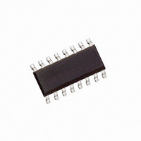
HCPL-090J-500 Avago Technologies US Inc., HCPL-090J-500 Datasheet - Page 12

HCPL-090J-500
Manufacturer Part Number
HCPL-090J-500
Description
ISOLATOR DGTL 4CH 100MBD 16-SOIC
Manufacturer
Avago Technologies US Inc.
Datasheet
1.HCPL-0900-000E.pdf
(14 pages)
Specifications of HCPL-090J-500
Inputs - Side 1/side 2
4/0
Number Of Channels
4
Isolation Rating
2500Vrms
Voltage - Supply
3 V ~ 5.5 V
Data Rate
100MBd
Propagation Delay
12ns
Output Type
CMOS
Package / Case
16-SOIC (3.9mm Width)
Operating Temperature
-40°C ~ 100°C
Operating Supply Voltage (typ)
3.3/5V
Lead Free Status / RoHS Status
Contains lead / RoHS non-compliant
Available stocks
Company
Part Number
Manufacturer
Quantity
Price
Company:
Part Number:
HCPL-090J-500E
Manufacturer:
AD
Quantity:
1 145
Applications Information
Power Consumption
The HCPL-90xx and HCPL-09xx CMOS digital isolators
achieves low power consumption from the manner by
which they transmit data across isolation barrier. By
detecting the edge transitions of the input logic signal
and converting this to a narrow current pulse, which
drives the isolation barrier, the isolator then latches the
input logic state in the output latch. Since the current
pulses are narrow, about 2.5 ns wide, the power consump-
tion is independent of mark-to-space ratio and solely
dependent on frequency.
The approximate power supply current per channel is:
I(Input) = 40(f/fmax)(1/4) mA
where f = operating frequency, fmax = 50 MHz.
Signal Status on Start-up and Shut Down
To minimize power dissipation, the input signals to the
channels of HCPL-90xx and HCPL-09xx digital isolators
are differentiated and then latched on the output side of
the isolation barrier to reconstruct the signal. This could
result in an ambiguous output state depending on power
up, shutdown and power loss sequencing. Therefore, the
designer should consider the inclusion of an initializa-
tion signal in this start-up circuit. Initialization consists of
toggling the input either high then low or low then high.
V
Figure 1. Functional Diagram of Single Channel HCPL-0900 or HCPL-0900.
GND
Figure 2. Recommended Printed Circuit Board Layout.
12
V
DD1
IN
DD1
Note: C1, C2 = 47 nF ceramic capacitors
IN
1
1
1
GND
C1
1
NC
1
2
3
4
C1
8
7
6
5
V
OE
GND
C2
2
V
OUT
DD2
1
V
OE
C2
Bypassing and PC Board Layout
The HCPL-90xx and HCPL-09xx digital isolators are
extremely easy to use. No external interface circuitry is
required because the isolators use high-speed CMOS IC
technology allowing CMOS logic to be connected directly
to the inputs and outputs. As shown in Figure 1, the only
external components required for proper operation are
two 47 nF ceramic capacitors for decoupling the power
supplies. For each capacitor, the total lead length between
both ends of the capacitor and the power-supply pins
should not exceed 20 mm. Figure 2 illustrates the recom-
mended printed circuit board layout for the HCPL-9000
or HCPL-0900. For data rates in excess of 10MBd, use of
ground planes for both GND
mended.
V
OUT
GND
DD2
1
2
1
and GND
2
is highly recom-


