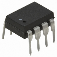
HCPL-4504-000E Avago Technologies US Inc., HCPL-4504-000E Datasheet - Page 18

HCPL-4504-000E
Manufacturer Part Number
HCPL-4504-000E
Description
OPTOCOUPLER TRANS-OUT 1MBD 8-DIP
Manufacturer
Avago Technologies US Inc.
Datasheet
1.HCPL-4504-000E.pdf
(19 pages)
Specifications of HCPL-4504-000E
Input Type
DC
Package / Case
8-DIP (0.300", 7.62mm)
Voltage - Isolation
3750Vrms
Number Of Channels
1, Unidirectional
Current - Output / Channel
8mA
Propagation Delay High - Low @ If
200ns @ 16mA
Current - Dc Forward (if)
25mA
Output Type
Open Collector
Mounting Type
Through Hole
Isolation Voltage
3750 Vrms
Maximum Continuous Output Current
8 mA
Maximum Forward Diode Current
25 mA
Output Device
Transistor With Base
Configuration
1 Channel
Current Transfer Ratio
65 %
Maximum Baud Rate
1 MBps
Maximum Forward Diode Voltage
1.7 V
Maximum Reverse Diode Voltage
5 V
Maximum Input Diode Current
25 mA
Maximum Power Dissipation
100 mW
Maximum Operating Temperature
+ 100 C
Minimum Operating Temperature
- 55 C
No. Of Channels
1
Optocoupler Output Type
Phototransistor
Input Current
16mA
Output Voltage
20V
Opto Case Style
DIP
No. Of Pins
8
Ctr Min
26%
Common Mode Ratio
10k
Rohs Compliant
Yes
Lead Free Status / RoHS Status
Lead free / RoHS Compliant
Lead Free Status / RoHS Status
Lead free / RoHS Compliant, Lead free / RoHS Compliant
Other names
516-1479-5
Available stocks
Company
Part Number
Manufacturer
Quantity
Price
Company:
Part Number:
HCPL-4504-000E
Manufacturer:
AVAGO
Quantity:
5 000
Company:
Part Number:
HCPL-4504-000E
Manufacturer:
AVAGO
Quantity:
97
Part Number:
HCPL-4504-000E/HCPL4504-000E
Manufacturer:
AVAGO/安华高
Quantity:
20 000
Figure 17. LED delay and dead time diagram.
Power Inverter Dead Time and Propagation Delay Specifi ca-
tions
The HCPL-4504/0454/J454 and HCNW4504 include a
specifi ca tion intended to help designers minimize “dead
time” in their power inverter designs. The new “propaga-
tion delay diff erence” specifi cation (t
deter min ing not only how much optocoupler switch-
ing delay is needed to prevent “shoot-through” current,
but also for determin ing the best achievable worst-case
dead time for a given design.
When inverter power transis tors switch (Q1 and Q2 in
Figure 17), it is essential that they never conduct at the
same time. Extremely large currents will fl ow if there is
any overlap in their conduction during switching tran-
sitions, poten tially damaging the transistors and even
the sur rounding circuitry. This “shoot-through” current is
eliminated by delay ing the turn-on of one transistor (Q2)
long enough to ensure that the opposing transistor (Q1)
has completely turned off . This delay intro duces a small
amount of “dead time” at the output of the inverter dur-
ing which both transistors are off during switching tran-
sitions. Minimiz ing this dead time is an important design
goal for an inverter designer.
18
PLH
- t
PHL
) is useful for
The amount of turn-on delay needed depends on the
propa ga tion delay characteristics of the optocoupler, as
well as the characteristics of the transistor base/gate drive
circuit. Consid er ing only the delay characteris tics of the
optocoupler (the charac teristics of the base/gate drive
circuit can be analyzed in the same way), it is important
to know the minimum and maximum turn-on (t
turnoff (t
ably over the desired operating temperature range. The
importance of these specifi cations is illustrated in Figure
17. The waveforms labeled “LED1”, “LED2”, “OUT1”, and
“OUT2” are the input and output voltages of the opto-
coupler circuits driving Q1 and Q2 respectively. Most in-
verters are designed such that the power transistor turns
on when the optocoupler LED turns on; this ensures that
both power transistors will be off in the event of a power
loss in the control circuit. Inverters can also be designed
such that the power transistor turns off when the opto-
coupler LED turns on; this type of design, however, re-
quires additional fail-safe circuitry to turn off the power
transistor if an over-current condition is detected. The
timing illustrated in Figure 17 assumes that the power
transistor turns on when the optocoupler LED turns on.
PLH
) propagation delay specifi ca tions, prefer-
PHL
) and


