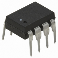
HCPL-3150 Avago Technologies US Inc., HCPL-3150 Datasheet - Page 19

HCPL-3150
Manufacturer Part Number
HCPL-3150
Description
OPTOCOUPLER GATE DRIVE 0.6A 8DIP
Manufacturer
Avago Technologies US Inc.
Datasheet
1.HCPL-3150.pdf
(21 pages)
Specifications of HCPL-3150
Voltage - Isolation
3750Vrms
Number Of Channels
1, Unidirectional
Current - Output / Channel
600mA
Propagation Delay High - Low @ If
300ns @ 7mA ~ 16mA
Current - Dc Forward (if)
25mA
Input Type
DC
Output Type
Open Collector
Mounting Type
Through Hole
Package / Case
8-DIP (0.300", 7.62mm)
No. Of Channels
1
Isolation Voltage
3.75kV
Optocoupler Output Type
Gate Drive
Input Current
16mA
Output Voltage
30V
Opto Case Style
DIP
No. Of Pins
8
Propagation Delay Low-high
0.5µs
Common Mode Voltage Vcm
1500V
Lead Free Status / RoHS Status
Contains lead / RoHS non-compliant
Other names
516-1125-5
Available stocks
Company
Part Number
Manufacturer
Quantity
Price
Company:
Part Number:
HCPL-3150
Manufacturer:
AVAGO
Quantity:
20 000
Part Number:
HCPL-3150
Manufacturer:
AGILENT
Quantity:
20 000
Company:
Part Number:
HCPL-3150#500
Manufacturer:
AGILENT
Quantity:
5 510
Company:
Part Number:
HCPL-3150#500
Manufacturer:
HIT
Quantity:
5 510
Company:
Part Number:
HCPL-3150#500
Manufacturer:
AVAGO
Quantity:
242
Part Number:
HCPL-3150#500
Manufacturer:
AGILENT
Quantity:
20 000
Company:
Part Number:
HCPL-3150-000E
Manufacturer:
AVAGO
Quantity:
20 000
Part Number:
HCPL-3150-000E
Manufacturer:
AVAGO/安华高
Quantity:
20 000
Part Number:
HCPL-3150-300E
Manufacturer:
AVAGO/安华高
Quantity:
20 000
Part Number:
HCPL-3150-360E
Manufacturer:
AVAGO/安华高
Quantity:
20 000
IPM Dead Time and Propagation Delay Specifications
The HCPL-3150/315J includes a Propagation Delay Dif-
ference (PDD) specification intended to help designers
minimize “dead time” in their power inverter designs.
Dead time is the time period during which both the high
and low side power transistors (Q1 and Q2 in Figure 25)
are off. Any overlap in Q1 and Q2 conduction will result
in large currents flowing through the power devices
from the high- to the low-voltage motor rails.
To minimize dead time in a given design, the turn on of
LED2 should be delayed (relative to the turn off of LED1)
so that under worst-case conditions, transistor Q1 has
just turned off when transistor Q2 turns on, as shown in
Figure 34. The amount of delay necessary to achieve this
condi tions is equal to the maximum value of the propa-
gation delay difference specification, PDD
specified to be 350 ns over the operating temperature
range of -40°C to 100°C.
Figure 29. Optocoupler Input to Output Capacitance Model for
Unshielded Optocouplers.
19
Figure 31. Equivalent Circuit for Figure 25 During Common Mode Transient.
+5 V
1
2
3
4
C
C
LEDP
LEDN
V
+
–
SAT
* THE ARROWS INDICATE THE DIRECTION
OF CURRENT FLOW DURING –dV
1
2
3
4
C
C
I
LEDP
LEDP
LEDN
SHIELD
8
7
6
5
V
+
CM
–
CM
/dt.
8
7
6
5
MAX
, which is
0.1
μF
+
–
Rg
V
Delaying the LED signal by the maximum propaga-
tion delay difference ensures that the minimum dead
time is zero, but it does not tell a designer what the
maximum dead time will be. The maximum dead
time is equivalent to the difference between the
maximum and minimum propa ga tion delay differ-
ence specifica tions as shown in Figure 35. The maxi-
mum dead time for the HCPL-3150/315J is 700 ns
(= 350 ns - (-350 ns)) over an operating temperature
range of -40°C to 100°C.
Note that the propagation delays used to calculate PDD
and dead time are taken at equal tempera tures and test
conditions since the optocouplers under consider ation
are typically mounted in close proximity to each other
and are switching identical IGBTs.
Figure 30. Optocoupler Input to Output Capacitance Model for
Shielded Optocouplers.
CC
1
2
3
4
= 18 V
• • •
• • •
C
C
LEDP
LEDN
C
SHIELD
LEDO1
C
LEDO2
8
7
6
5


