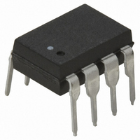
HCPL-3180-000E Avago Technologies US Inc., HCPL-3180-000E Datasheet - Page 14

HCPL-3180-000E
Manufacturer Part Number
HCPL-3180-000E
Description
OPTOCOUPLER 2.0A 250KHZ 8-DIP
Manufacturer
Avago Technologies US Inc.
Datasheet
1.HCPL-3180-000E.pdf
(16 pages)
Specifications of HCPL-3180-000E
Package / Case
8-DIP (0.300", 7.62mm)
Voltage - Isolation
3750Vrms
Number Of Channels
1, Unidirectional
Current - Output / Channel
2.5A
Propagation Delay High - Low @ If
150ns @ 10mA
Current - Dc Forward (if)
16mA
Input Type
DC
Output Type
Gate Driver
Mounting Type
Through Hole
Isolation Voltage
3750 Vrms
Maximum Fall Time
0.025 us
Maximum Forward Diode Current
25 mA
Minimum Forward Diode Voltage
1.2 V
Output Device
Integrated Photo IC
Configuration
1 Channel
Maximum Forward Diode Voltage
1.8 V
Maximum Reverse Diode Voltage
5 V
Maximum Power Dissipation
295 mW
Maximum Operating Temperature
+ 100 C
Minimum Operating Temperature
- 40 C
Number Of Elements
1
Forward Voltage
1.8V
Forward Current
25mA
Package Type
PDIP
Operating Temp Range
-40C to 100C
Power Dissipation
295mW
Propagation Delay Time
200ns
Pin Count
8
Mounting
Through Hole
Reverse Breakdown Voltage
5V
Operating Temperature Classification
Industrial
No. Of Channels
1
Optocoupler Output Type
Gate Drive
Input Current
16mA
Output Voltage
20V
Opto Case Style
DIP
No. Of Pins
8
Common Mode Ratio
10 KV/uS
Rohs Compliant
Yes
Lead Free Status / RoHS Status
Lead free / RoHS Compliant
Lead Free Status / RoHS Status
Lead free / RoHS Compliant, Lead free / RoHS Compliant
Other names
516-1674-5
Available stocks
Company
Part Number
Manufacturer
Quantity
Price
Company:
Part Number:
HCPL-3180-000E
Manufacturer:
AVAGO
Quantity:
6 236
Part Number:
HCPL-3180-000E
Manufacturer:
AVAGO/安华高
Quantity:
20 000
LED Drive Circuit Considerations for Ultra High CMR Performance
Without a detector shield, the dominant cause of op-
tocoupler CMR failure is capacitive coupling from the
input side of the optocoupler, through the package, to
the detector IC as shown in Figure 28. The HCPL-3180
improves CMR performance by using a detector IC with
an optically transparent Faraday shield, which diverts the
capacitively coupled current away from the sensitive IC
circuitry. However, this shield does not eliminate the ca-
pacitive coupling between the LED and optocoupler pins
5-8 as shown in Figure 29. This capacitive coupling causes
perturbations in the LED current during common mode
transients and becomes the major source of CMR failures
for a shielded optocoupler. The main design objective of
a high CMR LED drive circuit becomes keeping the LED in
the proper state (on or off ) during common mode tran-
sients. For example, the recommended application circuit
(Figure 25), can achieve 10 kV/µs CMR while minimizing
component complexity.
Techniques to keep the LED in the proper state are dis-
cussed in the next two sections.
Figure 29. Optocoupler input to output capacitance model for
shielded optocouplers.
14
Figure 28. Optocoupler input to output capacitance model for
unshielded optocouplers.
1
2
3
4
1
2
3
4
C
C
C
LEDP
LEDN
C
LEDN
LEDP
SHIELD
C
LEDO1
C
LEDO2
8
7
6
5
8
7
6
5
CMR with the LED On (CMR
A high CMR LED drive circuit must keep the LED on
during common mode transients. This is achieved by
over-driving the LED current beyond the input threshold
so that it is not pulled below the threshold during a
transient. A minimum LED current of 10 mA provides
adequate margin over the maximum I
8 mA to achieve 10 kV/µs CMR.
+5 V
CMR with the LED Off (CMR
A high CMR LED drive circuit must keep the LED off (V
≤ V
during a -dV
flowing through C
V
developed across the logic gate is less than V
LED will remain off and no common mode failure will
occur.
The open collector drive circuit, shown in Figure 31,
cannot keep the LED off during a +dV
since all the current flowing through C
supplied by the LED, and it is not recommended for ap-
plications requiring ultra high CMR
32 is an alternative drive circuit, which like the recom-
mended application circuit (Figure 25), does achieve
ultra high CMR performance by shunting the LED in the
off state.
Figure 30. Equivalent circuit for Figure 25 during common mode transient.
SAT
F(OFF)
of the logic gate. As long as the low state voltage
V
+
–
SAT
) during common mode transients. For example,
CM
1
2
3
4
* THE ARROWS INDICATE THE DIRECTION
OF CURRENT FLOW DURING –dV
/dt transient in Figure 30, the current
C
C
I
LEDP
LEDP
LEDN
LEDP
SHIELD
H
L
)
)
also flows through the R
+
V
CM
–
CM
/dt.
L
performance. Figure
8
7
6
5
FLH
CM
of
LEDN
/dt transient,
0.1
µF
F(OFF)
must be
SAT
+
–
, the
V
R
and
CC
g
= 20 V
F
• • •
• • •


