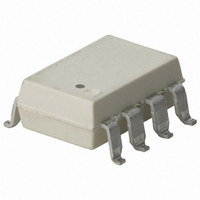
HCPL-3180-300E Avago Technologies US Inc., HCPL-3180-300E Datasheet - Page 12

HCPL-3180-300E
Manufacturer Part Number
HCPL-3180-300E
Description
OPTOCOUPLER 2.0A 250KHZ GW 8-SMD
Manufacturer
Avago Technologies US Inc.
Datasheet
1.HCPL-3180-000E.pdf
(16 pages)
Specifications of HCPL-3180-300E
Package / Case
8-SMD Gull Wing
Voltage - Isolation
3750Vrms
Number Of Channels
1, Unidirectional
Current - Output / Channel
2.5A
Propagation Delay High - Low @ If
150ns @ 10mA
Current - Dc Forward (if)
16mA
Input Type
DC
Output Type
Gate Driver
Mounting Type
Surface Mount
Isolation Voltage
3750 Vrms
Maximum Fall Time
0.025 us
Maximum Forward Diode Current
25 mA
Minimum Forward Diode Voltage
1.2 V
Output Device
Integrated Photo IC
Configuration
1 Channel
Maximum Forward Diode Voltage
1.8 V
Maximum Reverse Diode Voltage
5 V
Maximum Power Dissipation
295 mW
Maximum Operating Temperature
+ 100 C
Minimum Operating Temperature
- 40 C
Number Of Elements
1
Forward Voltage
1.8V
Forward Current
25mA
Package Type
PDIP SMD
Operating Temp Range
-40C to 100C
Power Dissipation
295mW
Propagation Delay Time
200ns
Pin Count
8
Mounting
Surface Mount
Reverse Breakdown Voltage
5V
Operating Temperature Classification
Industrial
No. Of Channels
1
Optocoupler Output Type
Gate Drive
Input Current
16mA
Output Voltage
20V
Opto Case Style
SMD
No. Of Pins
8
Propagation Delay Low-high
0.2µs
Rohs Compliant
Yes
Common Mode Ratio
10 KV/uS
Lead Free Status / RoHS Status
Lead free / RoHS Compliant
Lead Free Status / RoHS Status
Lead free / RoHS Compliant, Lead free / RoHS Compliant
Other names
516-1675-5
Available stocks
Company
Part Number
Manufacturer
Quantity
Price
Company:
Part Number:
HCPL-3180-300E
Manufacturer:
AVAGO
Quantity:
10 000
Part Number:
HCPL-3180-300E
Manufacturer:
AVAGO/安华高
Quantity:
20 000
Selecting the Gate Resistor (R
Step 1: Calculate R
R
by the HCPL-3180.
The V
2 A. (See Figure 6.)
Step 2: Check the HCPL-3180 power dissipation and increase R
The HCPL-3180 total power dissipation (P
power (P
For the circuit in Figure 25 with I
Cycle = 80%, Q
The value of 4.5 mA for I
the I
the P
tion.
For Q
12
g
in Figure 25 can be analyzed as a simple RC circuit with a voltage supplied
P
P
P
P
P
P
T
E
O
E
O
O(SWITCHING MAX)
CC
O(MAX)
OL
g
= P
= I
= P
= I
= 16 mA * 1.8 V * 0.8 = 23 mW
= 4.5 mA * 20 V + 0.85 µ * 200 kHz
= 260 mW ≥ 226 mW (P
= 100 nC, a value of E
max of 6 mA to I
value of 3 V in the previous equation is the V
E
F
CC
E
O(BIAS)
) and the output power (P
* V
E
+ P
, R
* V
SW(MAX)
F
g
O
CC
* Duty Cycle
g
must be increased to reduce the HCPL-3180 power dissipa-
+ P
= 100 nC, f = 200 kHz and T
+ E
g
O(SWITCHING)
minimum from the I
SW
R
g
CC
= P
= 226 mW – 90 mW
= 136 mW
= P
= 136 mW
= 0.68 µW
(R
CC
≥
=
= 8.5 Ω
g
) for HCPL-3180
g
V
200 kHz
max at +75°C. Since P
20 – 3
in the previous equation was obtained by derating
;Q
CC
O(MAX)
O(SWITCHING MAX)
sw
I
g
OLPEAK
– V
) * f
O(MAX)
2
= 0.68 µW gives a R
F
f
OL
(worst case) = 16 mA, R
– P
O
@ 75°C = 250 mW (5°C * 4.8 mW/°C))
).
O(BIAS)
OL
T
) is equal to the sum of the emitter
AMAX
peak specification. The IGBT and
O
= +75°C:
for this case is greater than
g
= 15 W.
OL
at the peak current of
g
= 10 Ω, Max Duty
g
if necessary.
Figure 26. Energy dissipated in the HCPL-3180 and for
each IGBT.
2.0
1.8
1.6
1.4
1.2
1.0
0.8
0.6
0.4
0.2
0
0
R
g
10
— GATE RESISTANCE — Ω
20
30
Q
g
= 100 nC
40
50


