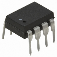
HCPL-3700-000E Avago Technologies US Inc., HCPL-3700-000E Datasheet

HCPL-3700-000E
Specifications of HCPL-3700-000E
Available stocks
Related parts for HCPL-3700-000E
HCPL-3700-000E Summary of contents
Page 1
... The HCPL-0370/3700 and HCPL-3760 are voltage/cur- rent threshold detection optocouplers. The HCPL-3760 is a low-current version of the HCPL-0370/3700. To obtain lower current operation, the HCPL-3760 uses a high-effi- ciency AlGaAs LED which provides higher light output at lower drive currents. The devices utilize threshold sens- ...
Page 2
... The HCPL-0370/3700’s input buffer IC has a nominal turn on threshold of 2 The buffer IC for the HCPL-3760 was redesigned to permit a lower input current. The nominal turn on threshold for the HCPL-3760 is 1 and 3.7 volts (V TH The high gain output stage features an open collector output providing both TTL compatible saturation voltages and CMOS compatible break down voltages ...
Page 3
... Schematic Package Outline Drawings Standard DIP Package (HCPL-3700/3760) 9.40 (0.370) 9.90 (0.390 XXXX YYWW PIN ONE 1.19 (0.047) MAX. 3.56 ± 0.13 (0.140 ± 0.005) 0.76 (0.030) 1.40 (0.056 TYPE NUMBER DATE CODE 6.10 (0.240) 6.60 (0.260) 7.36 (0.290) 7.88 (0.310) ...
Page 4
... Package Outline Drawings, continued Gull Wing Surface Mount Option 300 (HCPL-3700/3760) 9.65 ± 0.25 (0.380 ± 0.010 TYPE NUMBER DATE CODE A XXXX R U YYWW MOLDED 1.19 (0.047) MAX. 1.080 ± 0.320 (0.043 ± 0.013) 2.540 (0.100) BSC DIMENSIONS IN MILLIMETERS (INCHES). TOLERANCES (UNLESS OTHERWISE SPECIFIED): LEAD COPLANARITY MAXIMUM: 0 ...
Page 5
... T = 150 °C smax smin Note: Non-halide flux should be used. Regulatory Information The HCPL-0370/3700/3760 has been approved by the following organizations: IEC/EN/DIN EN 60747-5-5 (with option 060) Maximum Working Insulation Voltage V for HCPL-0370, and 630 Vpeak for HCPL3700/3760. Highest Allowable Overvoltage V IOTM HCPL-0370/3700/3760 ...
Page 6
... Insulation characteristics are guaranteed only within the safety maximum ratings, which must be ensured by protective circuits within the application. 2. Safety-limiting parameters are dependent on case temperature. The Input Current rate of 1.2 mA/°C and 1.53 mA/°C for HCPL-0370 and HCPL-3700/3760 respectively; the Output Power, P free-air case temperature at a rate of 4.8 mW/°C and 4 mW/°C for HCPL-0370 and HCPL-3700/3760 respectively. 6 ...
Page 7
... Solder Reflow Temperature Profile Recommended Operating Conditions Parameter Supply Voltage Operating Temperature Operating Frequency 7 Symbol Temperature Time Average Surge I IN Transient V IN HCPL-3700/3760 P IN HCPL-0370 HCPL-3700/3760 P T HCPL-0370 HCPL-3700/3760 P O HCPL-0370 Average See Package Outline Drawings section Symbol Min. Max Min. Max. Units ...
Page 8
... HYS Input Clamp V IHC1 Voltage V IHC2 V IHC3 V ILC Input Current I HCPL-0370/3700 IN HCPL-3760 Bridge Diode V HCPL-0370/3700 D1,2 Forward Voltage HCPL-3760 V HCPL-0370/3700 D3,4 HCPL-3760 Logic Low V OL Output Voltage Logic High I OH Output Current Logic Low I HCPL-0370/3700 CCL Supply Current HCPL-3760 Logic High I ...
Page 9
... Time to Logic Low t PHL at Output HCPL-3760 Propagation Delay HCPL-0370/3700 Time to Logic High t PLH at Output HCPL-3760 HCPL-0370/3700 Output Rise Time t r (10-90%) HCPL-3760 HCPL-0370/3700 Output Fall Time t f (90-10%) HCPL-3760 Common Mode Transient Immunity | Logic High Output Common Mode HCPL-0370/3700 Transient Immunity | ...
Page 10
... Derate linearly above 70°C free-air temperature at a rate of 5.4 mW/°C (HCPL-3700/3760) and 5 mW/°C (HCPL-0370). 6. Derate linearly above 70°C free-air temperature at a rate of 3.9 mW/°C (HCPL-3700/3760) and 1.9 mW/°C (HCPL-0370). Maximum output power dissipation of 210 mW (HCPL-3700/3760) and 103 mW (HCPL-0370) allows an output IC junction temperature of 125° ambient temperature 70° ...
Page 11
... T – TEMPERATURE – ° vs. temperature. OL HCPL-3700 fig 5b HCPL-3760 3.00 2.50 2.00 1.50 1.00 0.50 0 4.0 6.0 8.0 10.0 12.0 14.0 16.0 V – SUPPLY VOLTAGE – HCPL-370 fig 1.6 1 CCH OPEN 1 1.1 1.0 -3 0.9 10 0.8 0 0.6 0.5 0.4 ...
Page 12
... HCPL-3760 4.7 kΩ 5 5 PULSE WIDTH 100 µs (10-90 PLH PHL 2 0 -40 - – TEMPERATURE – °C A HCPL-3700 fig 7b HCPL-3760 30 700 25 600 20 500 15 400 4.7 kΩ 5 300 CC 5 PULSE WIDTH 100 Hz 5 200 µs (10-90 100 -40 - – TEMPERATURE – °C A ...
Page 13
Figure 10. Switching test circuit. Figure 11. Test circuit for common mode transient immunity and typical waveforms. Figure 12. Typical external threshold characteristics, V ± vs ...
Page 14
... R can provide over-current transient protection by X limiting input current during a transient condition. For monitoring con tacts of a relay or switch, the HCPL- 0370/3700/3760 in combina tion with R used to allow a specific current to be conducted through the contacts for clean ing purposes (wetting current). The choice of which input voltage clamp level to choose depends upon the application of this device (see Figure 1) ...


