HCPL-053L-000E Avago Technologies US Inc., HCPL-053L-000E Datasheet
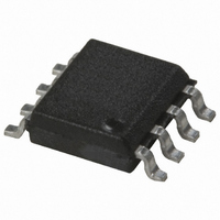
OPTOCOUPLER 1MBD 3.3V 8-SOIC

HCPL-053L-000E

Manufacturer Part Number
HCPL-053L-000E
Description
OPTOCOUPLER 1MBD 3.3V 8-SOIC
Manufacturer
Avago Technologies US Inc.
Datasheet

Specifications of HCPL-053L-000E

Input Type
DC
Package / Case
8-SOIC (0.154", 3.90mm Width)
Voltage - Isolation
3750Vrms
Number Of Channels
2, Unidirectional
Current - Output / Channel
8mA
Data Rate
1Mbps
Propagation Delay High - Low @ If
350ns @ 16mA
Current - Dc Forward (if)
25mA
Output Type
Open Collector
Mounting Type
Surface Mount
Isolation Voltage
3750 Vrms
Maximum Continuous Output Current
8 mA
Maximum Forward Diode Current
25 mA
Output Device
Transistor With Base
Configuration
2 Channel
Current Transfer Ratio
50 %
Maximum Baud Rate
1 MBps
Maximum Forward Diode Voltage
1.7 V
Maximum Reverse Diode Voltage
5 V
Maximum Input Diode Current
50 mA
Maximum Power Dissipation
100 mW
Maximum Operating Temperature
+ 85 C
Minimum Operating Temperature
0 C
Number Of Elements
2
Reverse Breakdown Voltage
5V
Forward Voltage
1.7V
Forward Current
50mA
Package Type
SOIC
Collector Current (dc) (max)
8mA
Power Dissipation
100mW
Pin Count
8
Mounting
Surface Mount
Operating Temp Range
0C to 85C
Operating Temperature Classification
Commercial
Lead Free Status / RoHS Status
Lead free / RoHS Compliant
Lead Free Status / RoHS Status
Lead free / RoHS Compliant, Lead free / RoHS Compliant
Other names
516-1632-5

Available stocks

Company
Part Number
Manufacturer
Quantity
Price
Part Number:
HCPL-053L-000E
Manufacturer:
AVAGO
Quantity:
40 000
HCPL-250L/050L/253L/053L
LVTTL/LVCMOS Compatible 3.3 V Optocouplers (1 Mb/s)
Data Sheet
Description
These diode-transistor optocouplers use an insulating
layer between a LED and an integrated photodetector
to provide electrical insulation between input and out-
put. Separate connections for the photodiode bias and
output-transistor collector increase the speed up to a
hundred times that of a conventional photo-transistor
coupler by reducing the base-collector capacitance.
These optocouplers are available in an 8-pin DIP and in
an industry standard SO-8 package. The following is a
cross reference table listing the 8-pin DIP part number
and the electrically equivalent SO-8 part number.
The SO-8 does not require "through holes" in a PCB. This
package occupies approximately one-third the foot-
print area of the standard dual-in-line package. The lead
profile is designed to be compatible with standard sur-
face mount processes.
These optocouplers can be used in LVTTL/LVCMOS or
wide bandwidth analog applications.
The common mode transient immunity of 1000 V/µs
minimum to typical at VCM = 10 V guaranteed for these
optocouplers.
8-Pin DIP
HCPL-250L
HCPL-253L
RoHS 6 fully compliant options available;
-xxxE denotes a lead-free product
Lead (Pb) Free
RoHS 6 fully
compliant
CAUTION: It is advised that normal static precautions be taken in handling and assembly
of this component to prevent damage and/or degradation which may be induced by ESD.
SO-8 Package
HCPL-050L
HCPL-053L
CATHODE
A 0.1 µF bypass capacitor must be connected between pins 5 and 8.
ANODE
NC
NC
Functional Diagram
Features
• 3.3V/5V Dual Supply Voltages
• Low power consumption
• High speed: 1 Mb/s
• LVTTL/LVCMOS compatible
• Available in 8-pin DIP, SO-8
• Open collector output
• Guaranteed performance from temperature:
• Safety approval, UL, CSA, IEC/EN/DIN EN 60747-5-2
Applications
• High voltage insulation
• Video signal isolation
• Power translator isolation in motor drives
• Line receivers
• Feedback element in switched mode power supplies
• High speed logic ground isolation – LVTTL/LVCMOS
• Replaces pulse transformers
• Replaces slow phototransistor isolators
HCPL–250L/HCPL–050L
1
2
3
4
0˚C to +70˚C
HCPL-250L Functional Diagram
8
7
6
5
V
V
V
GND
CC
B
O
(POSITIVE LOGIC)
LED
OFF
TRUTH TABLE
ON
CATHODE
CATHODE
HIGH
LOW
V
ANODE
ANODE
O
1
1
2
2
HCPL–253L/HCPL–053L
1
2
3
4
8
7
6
5
V
V
V
GND
CC
O1
O2

Related parts for HCPL-053L-000E

HCPL-053L-000E Summary of contents

Page 1

... Replaces slow phototransistor isolators Functional Diagram HCPL–250L/HCPL–050L ANODE CATHODE GND TRUTH TABLE (POSITIVE LOGIC) LED ON OFF A 0.1 µF bypass capacitor must be connected between pins 5 and 8. HCPL-250L Functional Diagram HCPL–253L/HCPL–053L ANODE CATHODE CATHODE ANODE 4 5 GND LOW ...

Page 2

... To order, choose a part number from the part number column and combine with the desired option from the option column to form an order entry. Example 1: HCPL-253L-560E to order product of 300 mil DIP Gull Wing Surface Mount package in Tape and Reel packaging with IEC/EN/DIN EN 60747-5-2 Safety Approval and RoHS compliant. Example 2: HCPL-253L to order product of 300 mil DIP package in Tube packaging and non RoHS compliant ...

Page 3

... Schematic HCPL - 250L / HCPL - 050L HCPL-250L/HCPL-050L ANODE + – CATHODE 3 SHIELD – GND – HCPL-253L/HCPL-053L GND 5 SHIELD HCPL-250/253L Schematic ...

Page 4

Package Outline Drawings 8-Pin DIP Package 9.65 ± 0.25 (0.380 ± 0.010 TYPE NUMBER A XXXXZ YYWW 1.78 (0.070) MAX. 1.19 (0.047) MAX. 3.56 ± 0.13 (0.140 ± 0.005) 1.080 ...

Page 5

Solder Reflow Temperature Profile 300 PREHEATING RATE 3°C + 1°C/–0.5°C/SEC. REFLOW HEATING RATE 2.5°C ± 0.5°C/SEC. 200 2.5°C ± 0.5°C/SEC. 160°C 150°C 140°C 3°C + 1°C/–0.5°C 100 PREHEATING TIME 150° SEC. ROOM TEMPERATURE Note: ...

Page 6

Insulation and Safety Related Specifications Parameter Symbol Minimum External Air L (101) Gap (External Clearance) Minimum External Tracking L (102) (External Creepage) Minimum Internal Plastic Gap (Internal Clearance) Tracking Resistance CTI (Comparative Tracking Index) Isolation Group IEC/EN/DIN EN 60747-5-2Insulation Related ...

Page 7

Absolute Maximum Ratings Parameter Storage Temperature Operating Temperature Average Forward Input Current Peak Forward Input Current (50% duty cycle pulse width) Peak Transient Input Current (≤ 1 µs pulse width, 300 pps) Reverse LED Input Voltage (Pin 3-2) ...

Page 8

... Ratio HCPL-250L HCPL-053L HCPL-253L Logic Low V HCPL-050L OL Output Voltage HCPL-250L HCPL-053L HCPL-253L Logic High I OH Output Current Logic Low I HCPL-050L CCL Supply Current HCPL-250L HCPL-053L HCPL-253L Logic High I HCPL-050L CCH Supply Current HCPL-250L HCPL-053L HCPL-253L Input Forward V F Voltage Input Reverse ...

Page 9

Switching Specifications (AC) Over Recommended Temperature (T All typicals 3 25° Parameter Sym. Device Min. Typ.* Propagation t PHL Delay Time to Logic Low at Output Propagation t PLH Delay Time to ...

Page 10

Package Characteristics Over Recommended Temperature (T Parameter Sym. Device Input-Output V 8-Pin DIP ISO Momentary SO-8 Withstand Voltage** I 8-Pin DIP I-O Input-Output R 8-Pin DIP I-O Resistance SO-8 Input-Output C 8-Pin DIP I-O Capacitance SO-8 *All typicals at T ...

Page 11

... T – TEMPERATURE – °C A Figure 2. Current transfer ratio vs. temperature. HCPL 250L Figure 2 8 PIN DIP, SO-8 Figure 5. Logic high output current vs. temperature 8 PIN DIP, SO-8 80 100 Figure 3. Current transfer ratio vs. temperature 8 PIN DIP, SO-8 800 P (mW) S 700 I ...

Page 12

... Avago, Avago Technologies, and the A logo are trademarks of Avago Technologies Limited in the United States and other countries. Data subject to change. Copyright © 2008 Avago Technologies Limited. All rights reserved. AV02-1200EN - May 5, 2008 I PULSE F 1 GEN 50Ω 10% DUTY CYCLE 1/f < 100 µ MONITOR HCPL-250L Figure – PULSE GEN. www.avagotech.com Obsoletes AV01-0549EN 8 ...

Related keywords