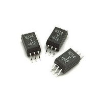
ACPL-W314-500E Avago Technologies US Inc., ACPL-W314-500E Datasheet

ACPL-W314-500E
Specifications of ACPL-W314-500E
Available stocks
Related parts for ACPL-W314-500E
ACPL-W314-500E Summary of contents
Page 1
... High speed response. x Ultra high CMR. x Bootstrappable supply current. x Available in Stretched SO-6 package x Package Clearance/Creepage at 8mm (ACPL-W314) x Safety Approval: UL1577 recognized with 3750 Vrms for 1 minute for ACPL-P314 and 5000 Vrms for 1 minute for ACPL- W314. CSA Approved. IEC/EN/DIN EN 60747-5-2 Approved V IORM V ...
Page 2
... Ordering Information ACPL-P314 is UL Recognized with 3750 Vrms for 1 minute per UL1577. ACPL-W314 is UL Recognized with 5000 Vrms for 1 minute per UL1577. Option Part number RoHS Compliant -000E -500E ACPL-P314 -060E -560E -000E -500E ACPL-W314 -060E -560E To order, choose a part number from the part number column and combine with the desired option from the option column to form an order entry ...
Page 3
... NOM. 1 ±0.250 [0.040 ±0.010] 9.7±0.250 [0.382 ±0.010] ACPL-W314 Stretched SO-6 Package 0.381 ± 0.127 [0.015 ± 0.005 7.62 [0.300] +0.127 6.807 0 +0.005 0.268 -0.000 45° 0.45 [0.018] 0.20± ...
Page 4
... Recommended Pb-Free IR Profile Recommended reflow condition as per JEDEC Standard, J-STD-020 (latest revision). Non-Halide Flux should be used. Regulatory Information The ACPL-P314/W314 is approved by the following organizations: IEC/EN/DIN EN 60747-5-2 (Option 060 only) Approval under: IEC 60747-5-5:2007 Table 1. IEC/EN/DIN EN 60747-5-2 Insulation Related Characteristics Description Installation classification per DIN VDE 0110/1.89, Table 1 ...
Page 5
... Maximum pulse width = 10 Ps, maximum duty cycle = 0.2%. This value is intended to allow for component tolerances for designs with I minimum = 0.4 A. See Application section for additional details on limiting I 3. Derate linearly above 85°C, free air temperature at the rate of 4.0 mW/°C. 4. Input power dissipation does not require derating. 5 ACPL- P314 W314 Unit Conditions 7 ...
Page 6
Table 5. Electrical Specifications (DC) Over recommended operating conditions unless otherwise specified. Parameter High Level Output Current Low Level Output Current High Level Output Voltage Low Level Output Voltage High Level Supply Current Low Level Supply Current Threshold Input Current ...
Page 7
... Table 7. Package Characteristics Parameter Input-Output ACPL-P314 Momentary ACPL-W314 Withstand Voltage Input-Output Resistance Input-Output Capacitance Notes accordance with UL 1577, each optocoupler is proof tested by applying an insulation test voltage > 4500 V < 5 PA). This test is performed before 100% production test for partial discharge (method B) shown in the IEC/EN/DIN EN ...
Page 8
T – TEMPERATURE – °C A Figure 1. V vs. Temperature 0.2 0.4 I – OUTPUT HIGH CURRENT – ...
Page 9
-50 - 100 T – TEMPERATURE – °C A Figure 7. I vs. Temperature. CC 3.5 3.0 2.5 2.0 1.5 -50 - ...
Page 10
T PLH 300 T PHL 250 200 0 50 100 150 Rg – SERIES LOAD RESISTANCE – Figure 13. Propagation Delay vs. Rg ...
Page 11
... Since P for this case is less than P O alright for the power dissipation. 4.0 3.5 at 3.0 OL 2.5 2.0 1.5 1.0 0 – GATE RESISTANCE – Figure 20. Energy Dissipated in the ACPL-P314/W314 and for Each IGBT Switching Cycle 24V 0 necessary. The ACPL-P314/W314 total ) is equal to the sum of the emitter T ) ...
Page 12
... Without a detector shield, the dominant cause of opto- coupler CMR failure is capacitive coupling from the input side of the optocoupler, through the package, to the detector IC as shown in Figure 21. The ACPL-P314/W314 improves CMR performance by using a detector IC with an optically transparent Faraday shield, which diverts the capacitively coupled current away from the sensitive IC circuitry ...
Page 13
... The maximum dead time is equivalent the difference between the maximum and minimum propagation delay difference specification as shown Figure 27. The maximum dead time for the ACPL-P314/ W314 is 1 μs (= 0.5 μs - (-0.5 μs)) over the operating tem- perature range of –40°C to 100°C. I LED1 V OUT1 ...
Page 14
... Thermal Model for ACPL-P314/W314 Streched-SO6 Pack- age Optocoupler Definitions R : Junction to Ambient Thermal Resistance of LED due 11 to heating of LED R : Junction to Ambient Thermal Resistance of LED due 12 to heating of Detector (Output IC Junction to Ambient Thermal Resistance of Detec- 21 tor (Output IC) due to heating of LED Junction to Ambient Thermal Resistance of Detec- ...


