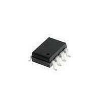
HCPL-3180-500 Avago Technologies US Inc., HCPL-3180-500 Datasheet - Page 4

HCPL-3180-500
Manufacturer Part Number
HCPL-3180-500
Description
OPTOCOUPLER DRVR 2.5A 8-SMD
Manufacturer
Avago Technologies US Inc.
Datasheet
1.HCPL-3180-000E.pdf
(16 pages)
Specifications of HCPL-3180-500
Package / Case
8-SMD Gull Wing
Voltage - Isolation
3750Vrms
Number Of Channels
1, Unidirectional
Current - Output / Channel
2.5A
Propagation Delay High - Low @ If
150ns @ 10mA
Current - Dc Forward (if)
16mA
Input Type
DC
Output Type
Gate Driver
Mounting Type
Surface Mount
Isolation Voltage
3750 Vrms
Maximum Fall Time
25 ns
Maximum Forward Diode Current
25 mA
Maximum Rise Time
25 ns
Minimum Forward Diode Voltage
1.2 V
Output Device
Integrated Photo IC
Configuration
1 Channel
Maximum Forward Diode Voltage
1.8 V
Maximum Reverse Diode Voltage
5 V
Maximum Power Dissipation
295 mW
Maximum Operating Temperature
+ 100 C
Minimum Operating Temperature
- 40 C
Lead Free Status / RoHS Status
Contains lead / RoHS non-compliant
Available stocks
Company
Part Number
Manufacturer
Quantity
Price
Company:
Part Number:
HCPL-3180-500
Manufacturer:
AVAGO
Quantity:
10 000
Company:
Part Number:
HCPL-3180-500E
Manufacturer:
AVAGO
Quantity:
10 000
Part Number:
HCPL-3180-500E
Manufacturer:
AVAGO/安华高
Quantity:
20 000
Recommended Pb-Free IR Profile
IEC/EN/DIN EN 60747-5-2 Insulation Characteristics (HCPL-3180 Option 060)
Description
* Refer to the optocoupler section of the Isolation and Control Components Designer’s Catalog, under Product Safety Regulations section IEC/
** Refer to the following figure for dependence of P
4
Partial Discharge < 5 pC
Installation classification per DIN EN 0110 1997-04
for rated mains voltage ≤ 150 V
for rated mains voltage ≤ 300 V
for rated mains voltage ≤ 600 V
Climatic Classification
Pollution Degree (DIN EN 0110 1997-04)
Maximum Working Insulation Voltage
Input to Output Test Voltage, Method b*
V
t
Input to Output Test Voltage, Method a*
V
Highest Allowable Overvoltage
(Transient Overvoltage t
Safety-limiting values – maximum values allowed in the
event of a failure.
Case Temperature
Input Current**
Output Power**
Insulation Resistance at T
Note: Non-halide flux should be used.
NOTES:
THE TIME FROM 25 °C to PEAK TEMPERATURE = 8 MINUTES MAX.
T
m
EN/DIN EN 60747-5-2 for a detailed description of Method a and Method b partial discharge test profiles.
IORM
IORM
smax
T
=1 sec, Partial Discharge < 5 pC
T
smax
smin
25
T
T
= 200 °C, T
p
L
x 1.875=V
x 1.5=V
217 °C
150 - 200 °C
smin
PR
t 25 °C to PEAK
, Type and Sample Test, t
PR
60 to 180 SEC.
3 °C/SEC. MAX.
= 150 °C
PREHEAT
, 100% Production Test with
t
RAMP-UP
s
260 +0/-5 °C
ini
S
, V
= 10 sec)
TIME
IO
= 500 V
rms
rms
rms
t
t
L
p
m
=60 sec,
TIME WITHIN 5 °C of ACTUAL
PEAK TEMPERATURE
20-40 SEC.
60 to 150 SEC.
S
RAMP-DOWN
6 °C/SEC. MAX.
and I
S
on ambient temperature.
Regulatory Information
The HCPL-3180 has been approved by the following
organizations:
IEC/EN/DIN EN 60747-5-2
Approved under: IEC 60747-5-2:1997 + A1:2002
EN 60747-5-2:2001 + A1:2002
DIN EN 60747-5-2 (VDE 0884 Teil 2):2003-01
(Option 060 only)
UL
Approval under UL 1577, component recognition
program up to V
CSA
Approval under CSA Component Acceptance Notice #5,
File CA 88324.
P
S, OUTPUT
I
Symbol
V
S,INPUT
V
V
V
IORM
IOTM
T
R
PR
PR
S
S
ISO
= 3750 V
55/100/21
HCPL-3180
rms
1181
6000
>10
I - IV
I - III
630
945
175
230
600
I-II
2
. File E55361.
9
V
V
V
V
mW
Unit
mA
peak
peak
peak
peak
°C
Ω


