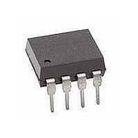
HCNW2611#500 Avago Technologies US Inc., HCNW2611#500 Datasheet

HCNW2611#500
Specifications of HCNW2611#500
Available stocks
Related parts for HCNW2611#500
HCNW2611#500 Summary of contents
Page 1
HCNW137, HCNW2601, HCNW2611, HCPL-0600, HCPL-0601, HCPL-0611, HCPL-0630, HCPL-0631, HCPL-0661, HCPL-2601, HCPL-2611, HCPL-2630, HCPL-2631, HCPL-4661 High CMR, High Speed TTL Compatible Optocouplers Data Sheet Lead (Pb) Free RoHS 6 fully compliant RoHS 6 fully compliant options available; -xxxE denotes a ...
Page 2
The 6N137, HCPL-26XX, HCPL-06XX, HCPL-4661, HCNW137, and HCNW26X1 are suitable for high speed logic interfac- ing, input/output buffering, as line receivers in environ- ments that conventional line receivers cannot tolerate and are recom mended for use in extremely high ground ...
Page 3
Ordering Information HCPL-xxxx is UL Recognized with 3750 Vrms for 1 minute per UL1577. HCNWxxxx is UL Rcognized with 5000 Vrms for 1 minute per UL1577. Option Part RoHS Non RoHS Number Compliant Compliant -000E No option -300E #300 -500E ...
Page 4
Option Part RoHS Non RoHS Number Compliant Compliant -000E No option HCPL-0600 -500E #500 HCPL-0601 HCPL-0611 -060E #060 -560E #560 HCPL-0630 -000E No option HCPL-0631 -500E #500 HCPL-0661 -000E No option HCNW137 HCNW2601 -300E #300 HCNW2611 -500E #500 To order, ...
Page 5
Package Outline Drawings 8-pin DIP Package** (6N137, HCPL-2601/11/30/31, HCPL-4661) 9.65 ± 0.25 (0.380 ± 0.010 TYPE NUMBER A XXXXZ YYWW 1.19 (0.047) MAX. 3.56 ± 0.13 (0.140 ± 0.005) 1.080 ± 0.320 (0.043 ...
Page 6
Small-Outline SO-8 Package (HCPL-0600/01/11/30/31/61 XXX 3.937 ± 0.127 YWW (0.155 ± 0.005 PIN ONE 0.406 ± 0.076 (0.016 ± 0.003) * 5.080 ± 0.127 (0.200 ± 0.005) 3.175 ± 0.127 (0.125 ± 0.005) TOTAL ...
Page 7
Widebody DIP Package with Gull Wing Surface Mount Option 300 (HCNW137, HCNW2601/11) 11.23 ± 0.15 (0.442 ± 0.006 1.80 ± 0.15 (0.071 ± 0.006) 2.54 (0.100) BSC DIMENSIONS IN MILLIMETERS (INCHES). LEAD COPLANARITY ...
Page 8
Recommended Pb-free IR Profile * 260 +0/-5 ° 217 ° RAMP-UP 3 °C/SEC. MAX. 150 - 200 °C T smax T smin t s PREHEAT 60 to 180 SEC °C to PEAK TIME ...
Page 9
IEC/EN/DIN EN 60747-5-2 Insulation Related Characteristics (HCPL-06xx Option 060 Only) Description Installation classification per DIN VDE 0110/1.89, Table 1 for rated mains voltage ≤ 150 V rms for rated mains voltage ≤ 300 V rms for rated mains voltage ≤ ...
Page 10
IEC/EN/DIN EN 60747-5-2 Insulation Related Characteristics (HCPL-26xx; 46xx; 6N13x Option 060 Only) Description Installation classification per DIN VDE 0110/1.89, Table 1 for rated mains voltage ≤ 300 V rms for rated mains voltage ≤ 450 V rms Climatic Classification Pollution ...
Page 11
Absolute Maximum Ratings* (No Derating Required up to 85°C) Parameter Storage Temperature Operating Temperature† Average Forward Input Current Reverse Input Voltage Input Power Dissipation Supply Voltage (1 Minute Maximum) Enable Input Voltage (Not to Exceed V by more than CC ...
Page 12
Electrical Specifications Over recommended temperature (T All enable test conditions apply to single channel products only. See note 5. Parameter Sym. Package High Level Output Current Input Threshold I Single Channel TH Current Widebody Dual Channel Low ...
Page 13
Switching Specifications (AC) Over Recommended Temperature (T All Typicals 25° Parameter Sym. Propagation Delay t PLH Time to High Output Level Propagation Delay t PHL Time to Low Output Level Pulse ...
Page 14
Package Characteristics All Typicals 25°C. A Parameter Sym. Package Input-Output I * Single 8-Pin DIP I-O Insulation Single SO-8 Input-Output V 8-Pin DIP, SO-8 ISO Momentary With- Widebody stand Voltage** OPT 020† Input-Output R 8-Pin DIP, SO-8 ...
Page 15
250 μ FOR SINGLE CHANNEL PRODUCTS ONLY 5 0 -60 -40 - 100 T ...
Page 16
DIP, SO FOR SINGLE 2.0 V* CHANNEL 0 5.0 mA PRODUCTS ONLY F 0 0.4 0.3 ...
Page 17
SINGLE CHANNEL I F PULSE GEN Ω INPUT 3 MONITORING NODE GND Figure 8. Test circuit for t and t . ...
Page 18
PULSE GEN Ω INPUT V E MONITORING NODE 7 GND Figure 13. Test circuit for ...
Page 19
HCPL-2611 OPTION 060 800 P (mW) S 700 I (mA) S 600 500 400 300 200 100 100 125 150 175 200 T – CASE TEMPERATURE – °C S Figure 16. Thermal derating curve, dependence ...
Page 20
SINGLE CHANNEL DEVICE CC1 470 Ω D1 – GND 1 SHIELD 1 *DIODE D1 (1N916 OR EQUIVALENT) IS NOT REQUIRED FOR UNITS WITH OPEN COLLECTOR OUTPUT. DUAL CHANNEL DEVICE CHANNEL ...
Page 21
Propagation Delay, Pulse-Width Distortion and Propagation Delay Skew Propagation delay is a figure of merit which describes how quickly a logic signal propagates through a sys- tem. The propaga tion delay from low to high (t amount of time required ...
Page 22
For product information and a complete list of distributors, please go to our website: Avago, Avago Technologies, and the A logo are trademarks of Avago Technologies Limited in the United States and other countries. Data subject to change. Copyright © ...


