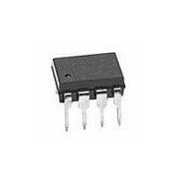
HCPL-3180-360E Avago Technologies US Inc., HCPL-3180-360E Datasheet - Page 12

HCPL-3180-360E
Manufacturer Part Number
HCPL-3180-360E
Description
OPTOCOUPLER DRV 2.5A VDE 8SMD GW
Manufacturer
Avago Technologies US Inc.
Datasheet
1.HCPL-3180-000E.pdf
(16 pages)
Specifications of HCPL-3180-360E
Voltage - Isolation
3750Vrms
Number Of Channels
1, Unidirectional
Current - Output / Channel
2.5A
Propagation Delay High - Low @ If
150ns @ 10mA
Current - Dc Forward (if)
16mA
Input Type
DC
Output Type
Gate Driver
Mounting Type
Surface Mount
Package / Case
8-SMD Gull Wing
No. Of Channels
1
Optocoupler Output Type
Gate Drive
Input Current
16mA
Output Voltage
20V
Opto Case Style
SMD
No. Of Pins
8
Propagation Delay Low-high
0.2µs
Isolation Voltage
3.75kV
Number Of Elements
1
Forward Voltage
1.8V
Forward Current
25mA
Package Type
PDIP SMD
Operating Temp Range
-40C to 100C
Power Dissipation
295mW
Propagation Delay Time
200ns
Pin Count
8
Mounting
Surface Mount
Reverse Breakdown Voltage
5V
Operating Temperature Classification
Industrial
Lead Free Status / RoHS Status
Lead free / RoHS Compliant
Lead Free Status / RoHS Status
Lead free / RoHS Compliant, Lead free / RoHS Compliant
Available stocks
Company
Part Number
Manufacturer
Quantity
Price
Company:
Part Number:
HCPL-3180-360E
Manufacturer:
AVAGO
Quantity:
10 000
Part Number:
HCPL-3180-360E
Manufacturer:
AVAGO/安华高
Quantity:
20 000
Selecting the Gate Resistor (R
Step 1: Calculate R
R
by the HCPL-3180.
The V
2 A. (See Figure 6.)
Step 2: Check the HCPL-3180 power dissipation and increase R
The HCPL-3180 total power dissipation (P
power (P
For the circuit in Figure 25 with I
Cycle = 80%, Q
The value of 4.5 mA for I
the I
the P
tion.
For Q
12
g
in Figure 25 can be analyzed as a simple RC circuit with a voltage supplied
P
P
P
P
P
P
T
E
O
E
O
O(SWITCHING MAX)
CC
O(MAX)
OL
g
= P
= I
= P
= I
= 16 mA * 1.8 V * 0.8 = 23 mW
= 4.5 mA * 20 V + 0.85 µ * 200 kHz
= 260 mW ≥ 226 mW (P
= 100 nC, a value of E
max of 6 mA to I
value of 3 V in the previous equation is the V
E
F
CC
E
O(BIAS)
) and the output power (P
* V
E
+ P
, R
* V
SW(MAX)
F
g
O
CC
* Duty Cycle
g
must be increased to reduce the HCPL-3180 power dissipa-
+ P
= 100 nC, f = 200 kHz and T
+ E
g
O(SWITCHING)
minimum from the I
SW
R
g
CC
= P
= 226 mW – 90 mW
= 136 mW
= P
= 136 mW
= 0.68 µW
(R
CC
≥
=
= 8.5 Ω
g
) for HCPL-3180
g
V
200 kHz
max at +75°C. Since P
20 – 3
in the previous equation was obtained by derating
;Q
CC
O(MAX)
O(SWITCHING MAX)
sw
I
g
OLPEAK
– V
) * f
O(MAX)
2
= 0.68 µW gives a R
F
f
OL
(worst case) = 16 mA, R
– P
O
@ 75°C = 250 mW (5°C * 4.8 mW/°C))
).
O(BIAS)
OL
T
) is equal to the sum of the emitter
AMAX
peak specification. The IGBT and
O
= +75°C:
for this case is greater than
g
= 15 W.
OL
at the peak current of
g
= 10 Ω, Max Duty
g
if necessary.
Figure 26. Energy dissipated in the HCPL-3180 and for
each IGBT.
2.0
1.8
1.6
1.4
1.2
1.0
0.8
0.6
0.4
0.2
0
0
R
g
10
— GATE RESISTANCE — Ω
20
30
Q
g
= 100 nC
40
50


