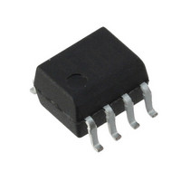
ACPL-054L-000E Avago Technologies US Inc., ACPL-054L-000E Datasheet

ACPL-054L-000E
Specifications of ACPL-054L-000E
ACPL-054L
Available stocks
Related parts for ACPL-054L-000E
ACPL-054L-000E Summary of contents
Page 1
... Feedback Elements in Switching Power Supplies 6 x Digital isolation for A/D, D/A conversion Digital field 5 Truth Table LED LOW 7 OFF HIGH 6 The connection of a 0.1 PF bypass capacitor between pins 5 4 and 6 for ACPL-M50L/W50L and between pins 5 and 8 for ACPL-054L/K54L is recommended. Operation CC = 1500 V CM ...
Page 2
... To order, choose a part number from the part number column and combine with the desired option from the option column to form an order entry. Example 1: ACPL-M50L-500E to order product of Mini-flat Surface Mount 5-pin package in Tape and Reel packaging with RoHS compliant. Option datasheets are available. Contact your Avago sales representative or authorized distributor for information. ...
Page 3
... Package Outline Drawings ACPL-M50L Small Outline SO-5 Package (JEDEC MO-155) M50L 4.4 ± 0.1 YWW (0.276 ± 0.008) (0.173 ± 0.004) 0.4 ± 0.05 (0.016 ± 0.002) 3.6 ± 0.1* (0.142 ± 0.004) 0.102 ± 0.102 2.5 ± 0.1 (0.004 ± 0.004) (0.098 ± ...
Page 4
... ACPL-054L (Small Outline S0-8 Package 54L x YWW 3.937 ± 0.127 (0.155 ± 0.005 PIN ONE 0.406 ± 0.076 (0.016 ± 0.003) * 5.080 ± 0.127 (0.200 ± 0.005) 3.175 ± 0.127 (0.125 ± 0.005) Total package length (inclusive of mold flash) * 5.207 ± 0.254 (0.205 ± 0.010) Dimensions in Millimeters (Inches) ...
Page 5
... Solder Reflow Profile Recommended reflow condition as per JEDEC Standard, J-STD-020 (latest revision). Non-Halide Flux should be used. Regulatory Information The ACPL-M50L/054L/W50L/K54L will be approved by the following organizations: UL Approval under UL 1577, component recognition program for ACPL-W50L/K54L. RMS CSA Approval under CSA Component Acceptance Notice #5 ...
Page 6
... Through insulation distance conductor to conductor, usually the straight line distance thickness between the emitter and detector. Volts DIN IEC 112/VDE 0303 Part 1 Material Group (DIN VDE 0110, 1/89, Table 1) Symbol Characteristic ACPL-M50L/ ACPL-W50L/ 054L K54L I – – – III I – – – III I – ...
Page 7
Absolute Maximum Ratings Parameter Storage Temperature Operating Temperature Lead Soldering Cycle Temperature Time [1] Average Forward Input Current [2] Peak Forward Input Current (50% duty cycle, 1ms pulse width) Peak Transient Input Current (≤1Ps pulse width, 300ps) Reversed Input Voltage ...
Page 8
... Over recommended operating T = -40°C to 105°C, supply voltage (2.7V ≤ typicals are at T =25°C A Parameter Sym. Part Number Min. [1] Current Transfer CTR ACPL-M50L Ratio ACPL-054L Logic Low V OL Output Voltage Logic High I OH Output Current Logic Low I CCL/CH Supply Current per Channel ...
Page 9
... Switching Specifications (ACPL-M50L) Over recommended operating (T = -40° Parameter Symbol Min Propagation Delay Time to T PHL Logic Low at Output Propagation Delay Time to T PLH Logic High at Output [1] Pulse Width Distortion PWD Propagation Delay t psk Difference Between [2] Any two Parts Common Mode Transient ...
Page 10
... Switching Specifications (ACPL-054L) Over recommended operating (T = -40° Parameter Symbol Min Propagation Delay Time to T PHL Logic Low at Output Propagation Delay Time to T PLH Logic High at Output Pulse Width PWD [1] Distortion Propagation Delay t psk Difference Between [2] Any two Parts Common Mode Transient ...
Page 11
... Input-Input Capacitance Notes: 1. Device considered a two terminal device: pins 1 and 3 shorted together and pins 4, 5 and 6 shorted together for ACPL-M50L, pins and 4 shorted together and pins and 8 shorted together for ACPL-054L/K54L, pins 1, 2 and 3 shorted together and pins 4, 5 and 6 shorted together for ACPL-W50L accordance with UL 1577, each optocoupler is proof tested by applying an insulation test voltage ≥ ...
Page 12
T = 25° 0.1 0.01 0.001 0.0001 1.1 1.2 1.3 1 FORWARD VOLTAGE - V F Figure 1. Input Current vs. Forward Voltage 1.1 1 0.9 0.8 NORMALIZED 0.7 ...
Page 13
... Figure 6b. Typical Propagation Delay vs. Temperature (ACPL-054L) 800 700 600 500 400 t PHL 300 200 100 100 120 Figure 7b. Typical Propagation Delay vs. Temperature (ACPL-054L) 600 500 t PHL 400 300 200 100 100 120 Figure 8b. Typical Propagation Delay vs. Temperature (ACPL-054L mA 3.3 V ...
Page 14
... PHL 1000 800 600 400 200 0 300 400 500 Figure 11b. Typical Propagation delay vs. Load Capacitance (ACPL-054L) 2500 kΩ R 2000 25°C A 1500 1000 500 Figure 12b. Typical Propagation Delay vs. Supply Voltage (ACPL-054L mA PLH t PHL 1 - LOAD RESISTANCE - kΩ mA 14.8 kΩ 25° PHL ...
Page 15
... V 90% 90% CM 10% 10 SWITCH SWITCH Figure 15. Test Circuit for Transient Immunity and typical waveforms 15 600 500 25°C A 400 300 200 100 Figure 13b. Typical Propagation Delay vs. Supply Current (ACPL-054L) PULSE I F GEN Ω MONITOR PULSE GEN PLH t PHL FORWARD LED CURRENT - ...
Page 16
150 100 FORWARD CURRENT - mA F Figure 16. Current Transfer Ratio versus Input Current For product information and a complete ...


