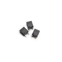
ACPL-M61T-000E Avago Technologies US Inc., ACPL-M61T-000E Datasheet - Page 9

ACPL-M61T-000E
Manufacturer Part Number
ACPL-M61T-000E
Description
OPTOCOUPLER 10MBD AUTO 5-SOIC
Manufacturer
Avago Technologies US Inc.
Datasheet
1.ACPL-M61T-000E.pdf
(10 pages)
Specifications of ACPL-M61T-000E
Isolation Voltage
3750 Vrms
Maximum Fall Time
10 ns
Maximum Rise Time
24 ns
Output Device
Logic Gate Photo IC
Configuration
1 Channel
Maximum Baud Rate
10 MBps
Maximum Forward Diode Voltage
1.95 V
Maximum Reverse Diode Voltage
5 V
Maximum Power Dissipation
85 mW
Maximum Operating Temperature
+ 100 C
Minimum Operating Temperature
- 40 C
Package / Case
SO-5
Number Of Elements
1
Input Type
DC
Output Type
Open Collector
Forward Voltage
1.75V
Forward Current
20mA
Output Current
50mA
Package Type
SOIC
Operating Temp Range
-40C to 125C
Power Dissipation
85mW
Propagation Delay Time
75ns
Pin Count
5
Mounting
Surface Mount
Reverse Breakdown Voltage
5V
Lead Free Status / RoHS Status
Lead free / RoHS Compliant
Lead Free Status / RoHS Status
Lead free / RoHS Compliant, Lead free / RoHS Compliant
Available stocks
Company
Part Number
Manufacturer
Quantity
Price
Company:
Part Number:
ACPL-M61T-000E
Manufacturer:
AVAGO
Quantity:
10 000
Part Number:
ACPL-M61T-000E
Manufacturer:
AVAGO/安华高
Quantity:
20 000
Propagation Delay, Pulse-Width Distortion and Propa-
gation Delay Skew
Propagation delay is a figure of merit which describes
how quickly a logic signal propagates through a system.
The propagation delay from low to high (t
amount of time required for an input signal to propagate
to the output, causing the output to change from low
to high. Similarly, the propagation delay from high to
low (t
signal to propagate to the output, causing the output to
change from high to low (see Figure 6).
Pulse-width distortion (PWD) results when t
differ in value. PWD is defined as the difference between
t
rate capability of a transmission system. PWD can be
expressed in percent by dividing the PWD (in ns) by
the minimum pulse width (in ns) being transmitted.
Typically, PWD on the order of 20-30% of the minimum
pulse width is tolerable; the exact figure depends on the
particular application (RS232, RS422, T-1, etc.).
Propagation delay skew, t
to consider in parallel data applications where synchro-
nization of signals on parallel data lines is a concern.
If the parallel data is being sent through a group of op-
tocouplers, differences in propagation delays will cause
the data to arrive at the outputs of the optocouplers at
different times. If this difference in propagation delays
is large enough, it will determine the maximum rate at
which parallel data can be sent through the optocou-
plers.
Propagation delay skew is defined as the difference
between the minimum and maximum propagation
delays, either t
couplers which are operating under the same conditions
(i.e., the same drive current, supply voltage, output load,
and operating temperature). As illustrated in Figure 14,
if the inputs of a group of optocouplers are switched
either ON or OFF at the same time, t
between the shortest propagation delay, either t
t
t
Figure 13. Recommended TTL/LSTTL to TTL/LSTTL Interface Circuit.
9
GND 1
PLH
PHL
PHL
V
CC
, and the longest propagation delay, either t
.
1
and t
PHL
5 V
) is the amount of time required for the input
1
PHL
* DIODE D1 (1N916 OR EQUIVALENT) IS NOT REQUIRED
FOR UNITS WITH OPEN COLLECTOR OUTPUT.
*D1
and often determines the maximum data
470
PLH
V
or t
F
I
F
PHL
1
3
PSK
, for any given group of opto-
, is an important parameter
SHIELD
PSK
is the difference
PLH
PLH
and t
) is the
PLH
PLH
4
5
6
PHL
or
or
0.1 μF
BYPASS
390 Ω
As mentioned earlier, t
parallel data transmission rate. Figure 15 is the timing
diagram of a typical parallel data application with both
the clock and the data lines being sent through opto-
couplers. The figure shows data and clock signals at the
inputs and outputs of the optocouplers. To obtain the
maximum data transmission rate, both edges of the clock
signal are being used to clock the data; if only one edge
were used, the clock signal would need to be twice as
fast.
Propagation delay skew represents the uncertainty of
where an edge might be after being sent through an op-
tocoupler. Figure 15 shows that there will be uncertainty
in both the data and the clock lines. It is important that
these two areas of uncertainty not overlap, otherwise the
clock signal might arrive before all of the data outputs
have settled, or some of the data outputs may start to
change before the clock signal has arrived. From these
considerations, the absolute minimum pulse width that
can be sent through optocouplers in a parallel applica-
tion is twice t
longer pulse width to ensure that any additional uncer-
tainty in the rest of the circuit does not cause a problem.
The t
of guaranteed specifications for propagation delays,
pulse-width distortion and propagation delay skew over
the recommended temperature, and input current, and
power supply ranges.
2
PSK
5 V
specified optocouplers offer the advantages
V
GND 2
PSK
CC
. A cautious design should use a slightly
2
PSK
can determine the maximum


