HCPL-J312-000E Avago Technologies US Inc., HCPL-J312-000E Datasheet - Page 24
HCPL-J312-000E
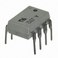
Manufacturer Part Number
HCPL-J312-000E
Description
OPTOCOUPLER 1CH 2.5A 8-DIP
Manufacturer
Avago Technologies US Inc.
Datasheet
1.HCPL-3120-500E.pdf
(24 pages)
Specifications of HCPL-J312-000E
Output Type
Gate Driver
Package / Case
8-DIP (0.300", 7.62mm)
Voltage - Isolation
3750Vrms
Number Of Channels
1, Unidirectional
Current - Output / Channel
2.5A
Propagation Delay High - Low @ If
300ns @ 7mA ~ 16mA
Current - Dc Forward (if)
16mA
Input Type
DC
Mounting Type
Through Hole
Configuration
1 Channel
Isolation Voltage
3750 Vrms
Maximum Propagation Delay Time
500 ns
Maximum Forward Diode Voltage
1.95 V
Minimum Forward Diode Voltage
1.2 V
Maximum Reverse Diode Voltage
3 V
Maximum Forward Diode Current
25 mA
Maximum Power Dissipation
295 mW
Maximum Operating Temperature
+ 100 C
Minimum Operating Temperature
- 40 C
No. Of Channels
1
Optocoupler Output Type
Gate Drive
Input Current
16mA
Output Voltage
30V
Opto Case Style
DIP
No. Of Pins
8
Common Mode Ratio
15 KV/uS
Rohs Compliant
Yes
Lead Free Status / RoHS Status
Lead free / RoHS Compliant
Lead Free Status / RoHS Status
Lead free / RoHS Compliant, Lead free / RoHS Compliant
Other names
516-1879-5
HCPL-J312-000E
HCPL-J312-000E
Available stocks
Company
Part Number
Manufacturer
Quantity
Price
Company:

Part Number:
HCPL-J312-000E
Manufacturer:
AVAGO
Quantity:
2 000
Part Number:
HCPL-J312-000E
Manufacturer:
AVAGO/安华高
Quantity:
20 000


To minimize dead time in a given design, the turn on of
LED2 should be delayed (relative to the turn off of LED1)
so that under worst-case con-ditions, transistor Q1 has
just turned off when transistor Q2 turns on, as shown in
Figure 35. The amount of delay necessary to achieve this
conditions is equal to the maximum value of the propa-
gation delay difference specification, PDD
specified to be 350 ns over the operating temperature
range of -40°C to 100°C.
Delaying the LED signal by the maximum propagation
delay difference ensures that the minimum dead time is
zero, but it does not tell a designer what the maximum
For product information and a complete list of distributors, please go to our website:
Avago, Avago Technologies, and the A logo are trademarks of Avago Technologies in the United States and other countries.
Data subject to change. Copyright © 2005-2008 Avago Technologies. All rights reserved. Obsoletes AV01-0622EN
AV02-0161EN - July 4, 2008
Figure 37. Thermal derating curve, dependence of safety limiting value with case temperature per IEC/EN/DIN EN 60747-5-2.
800
700
600
500
400
300
200
100
0
0
HCPL-3120 OPTION 060éHCPL-J312
T
25
S
– CASE TEMPERATURE – °C
50
HCPL-3120 fig 37a
P
I
OPTION 060
I
75 100
S
S
S
(mA) FOR HCPL-3120
(mA) FOR HCPL-J312
(mW)
125
150 175
200
1000
MAX
900
800
700
600
500
400
300
200
100
0
, which is
0
T
25
S
– CASE TEMPERATURE – °C
HCPL-3120 fig 37b
50
www.avagotech.com
P
I
S
HCNW3120
S
(mA)
(mW)
75
dead time will be. The maximum dead time is equivalent
to the difference between the maximum and minimum
propagation delay difference specifications as shown in
Figure 36. The maximum dead time for the HCPL-3120 is
700 ns (= 350 ns - (-350 ns)) over an operating tempera-
ture range of -40°C to 100°C.
Note that the propagation delays used to calculate PDD
and dead time are taken at equal temperatures and test
conditions since the optocouplers under consideration
are typically mounted in close proximity to each other
and are switching identical IGBTs.
100
125
150
175
Related parts for HCPL-J312-000E
Image
Part Number
Description
Manufacturer
Datasheet
Request
R

Part Number:
Description:
OPTOCOUPLER 1CH 2.5A 8-SMD
Manufacturer:
Avago Technologies US Inc.
Datasheet:

Part Number:
Description:
OPTOCOUPLER 1CH 2.5A 8-SMD GW
Manufacturer:
Avago Technologies US Inc.
Datasheet:
Part Number:
Description:
OPTOCOUPLER 1CH 2.5A 8-SMD GW
Manufacturer:
Avago Technologies US Inc.
Datasheet:

Part Number:
Description:
OPTOCOUPLER IGBT DRIVE 2A 8-DIP
Manufacturer:
Avago Technologies US Inc.
Datasheet:

Part Number:
Description:
OPTOCOUPLER 1CH 2.5A 8-SMD
Manufacturer:
Avago Technologies US Inc.
Datasheet:

Part Number:
Description:
OPTOCOUPLER GATE DRV 2A 16-SOIC
Manufacturer:
Avago Technologies US Inc.
Datasheet:
Part Number:
Description:
OPTOCOUPLER 2CH 2.5A 16-SOIC
Manufacturer:
Avago Technologies US Inc.
Datasheet:

Part Number:
Description:
OPTOCOUPLER GATE DRV 0.4A 16SOIC
Manufacturer:
Avago Technologies US Inc.
Datasheet:
Part Number:
Description:
OPTOCOUPLER 2.0A 250KHZ 8-DIP
Manufacturer:
Avago Technologies US Inc.
Datasheet:

Part Number:
Description:
OPTOCOUPLER 2.0A 250KHZ GW 8-SMD
Manufacturer:
Avago Technologies US Inc.
Datasheet:

Part Number:
Description:
OPTOCOUPLER 2CH 15MBD 3.3V 8SOIC
Manufacturer:
Avago Technologies US Inc.
Datasheet:
Part Number:
Description:
OPTOCOUPLER DARL-OUT 8-DIP
Manufacturer:
Avago Technologies US Inc.
Datasheet:
Part Number:
Description:
OPTOCOUPLER IGBT DRIVE 0.4A 8DIP
Manufacturer:
Avago Technologies US Inc.
Datasheet:
Part Number:
Description:
OPTOCOUPLER DARL-OUT 8-DIP
Manufacturer:
Avago Technologies US Inc.
Datasheet:

Part Number:
Description:
OPTOCOUPLER 1CH 1MBS 8-SMD GW
Manufacturer:
Avago Technologies US Inc.
Datasheet: