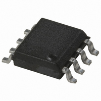
HCPL-0710 Avago Technologies US Inc., HCPL-0710 Datasheet - Page 10

HCPL-0710
Manufacturer Part Number
HCPL-0710
Description
OPTOCOUPLER CMOS 12MBD 8-SOIC
Manufacturer
Avago Technologies US Inc.
Datasheet
1.HCPL-7710-000E.pdf
(18 pages)
Specifications of HCPL-0710
Voltage - Isolation
3750Vrms
Number Of Channels
1, Unidirectional
Current - Output / Channel
10mA
Data Rate
12.5MBd
Propagation Delay High - Low @ If
20ns
Input Type
Logic
Output Type
Push-Pull, Totem-Pole
Mounting Type
Surface Mount
Package / Case
8-SOIC (0.154", 3.90mm Width)
No. Of Channels
1
Isolation Voltage
3.75kV
Optocoupler Output Type
Gate Drive
Input Current
10µA
Output Voltage
5V
Opto Case Style
SOIC
No. Of Pins
8
Propagation Delay Low-high
40ns
Common Mode Voltage Vcm
1000V
Lead Free Status / RoHS Status
Contains lead / RoHS non-compliant
Other names
516-1116-5
Available stocks
Company
Part Number
Manufacturer
Quantity
Price
Company:
Part Number:
HCPL-0710
Manufacturer:
AVAGO
Quantity:
18 000
Part Number:
HCPL-0710
Manufacturer:
AGILENT
Quantity:
20 000
Company:
Part Number:
HCPL-0710#000E
Manufacturer:
AVAGO
Quantity:
30 000
Company:
Part Number:
HCPL-0710#500
Manufacturer:
AGILENT
Quantity:
1 726
Company:
Part Number:
HCPL-0710#500E
Manufacturer:
AVAGO
Quantity:
21 000
Company:
Part Number:
HCPL-0710-000E
Manufacturer:
AVAGO
Quantity:
30 000
Part Number:
HCPL-0710-500
Manufacturer:
AVAGO/安华高
Quantity:
20 000
Part Number:
HCPL-0710-500E
Manufacturer:
AVAGO/安华高
Quantity:
20 000
10
Application Information
Bypassing and PC Board Layout
The HCPL-x710 optocouplers are extremely easy to
use. No external interface circuitry is required because
the HCPL-x710 use high-speed CMOS IC technology
allowing CMOS logic to be connected directly to the
inputs and outputs.
As shown in Figure 12, the only external components
Figure 12. Recommended Printed Circuit Board layout.
Figure 13. Recommended Printed Circuit Board layout.
Propagation Delay, Pulse-Width Distortion and Propagation Delay
Skew
Propagation Delay is a figure of merit which describes
how quickly a logic signal propagates through a
system. The propagation delay from low to high (t
is the amount of time required for an input signal to
propagate to the output, causing the output to change
Figure 14.
V
GND
INPUT
OUTPUT
V
DD1
DD1
V
V
1
I
V
I
V
O
I
GND
C1
1
10%
NC
C1, C2 = 0.01 µF TO 0.1 µF
C1
1
2
3
4
90%
HCPL-0710 fig 11
t
PLH
HCPL-0710 fig 13
t
PHL
8
7
6
5
HCPL-0710 fig 12
NC
90%
GND
50%
C2
10%
2
PLH
V
V
5 V CMOS
0 V
V
2.5 V CMOS
V
DD2
O
)
OH
OL
required for proper operation are two bypass capacitors.
Capacitor values should be between 0.01 µF and 0.1 µF.
For each capacitor, the total lead length between both
ends of the capacitor and the power-supply pins should
not exceed 20 mm. Figure 13 illustrates the recommend-
ed printed circuit board layout for the HPCL-x710.
from low to high. Similarly, the propagation delay from
high to low (t
input signal to propagate to the output, causing the
output to change from high to low. See Figure 14.
C2
C1, C2 = 0.01 µF TO 0.1 µF
PHL
) is the amount of time required for the
V
V
GND
DD2
O
2


