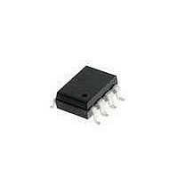
HCPL-263N#300 Avago Technologies US Inc., HCPL-263N#300 Datasheet - Page 14

HCPL-263N#300
Manufacturer Part Number
HCPL-263N#300
Description
OPTOCOUPLER 2CH 10MBD 8-SMD GW
Manufacturer
Avago Technologies US Inc.
Datasheet
1.HCPL-061A-000E.pdf
(17 pages)
Specifications of HCPL-263N#300
Package / Case
8-SMD Gull Wing
Voltage - Isolation
3750Vrms
Number Of Channels
2, Unidirectional
Current - Output / Channel
50mA
Data Rate
10MBd
Propagation Delay High - Low @ If
53ns @ 3.5mA
Current - Dc Forward (if)
10mA
Input Type
DC
Output Type
Open Collector
Mounting Type
Surface Mount, Gull Wing
Isolation Voltage
3750 Vrms
Maximum Continuous Output Current
50 mA
Maximum Fall Time
12 ns
Maximum Forward Diode Current
10 mA
Maximum Rise Time
42 ns
Minimum Forward Diode Voltage
1 V
Output Device
Logic Gate Photo IC
Configuration
2 Channel
Maximum Baud Rate
10 MBps
Maximum Forward Diode Voltage
1.6 V
Maximum Reverse Diode Voltage
3 V
Maximum Power Dissipation
60 mW
Maximum Operating Temperature
+ 85 C
Minimum Operating Temperature
- 40 C
Lead Free Status / RoHS Status
Contains lead / RoHS non-compliant
Available stocks
Company
Part Number
Manufacturer
Quantity
Price
Figure 19. Recommended printed circuit board layout.
Figure 20. Recommended drive circuit for HCPL-261A/-261N families for high-CMR (similar for HCPL-
263A/-263N).
14
OR ANY TOTEM-POLE
OUTPUT LOGIC GATE
*Higher CMR may be obtainable by connecting pins 1, 4 to input ground (Gnd1).
V
V
CC
CC
*
HIGHER CMR MAY BE OBTAINABLE BY CONNECTING PINS 1, 4 TO INPUT GROUND (GND1).
BUS (FRONT)
BUS (FRONT)
N.C.
N.C.
N.C.
N.C.
V CC
74LS04
GND1
(MAX.)
(MAX.)
357 Ω
357 Ω
0.1µF
0.1µF
0.1µF
SINGLE CHANNEL PRODUCTS
DUAL CHANNEL PRODUCTS
*
*
1
2
3
4
HCPL-261A fig 19
HCPL-261A/261N
SHIELD
10 mm MAX. (SEE NOTE 16)
GND BUS (BACK)
10 mm MAX. (SEE NOTE 16)
GND BUS (BACK)
8
7
6
5
ENABLE
(IF USED)
OUTPUT 1
ENABLE
(IF USED)
OUTPUT 2
0.01 µF
OUTPUT 1
OUTPUT 2
GND2
350 Ω
V CC+
V O
GND
Application Information
Common-Mode Rejection for HCPL-
261A/HCPL-261N Families:
Figure 20 shows the recommended
drive circuit for the HCPL-261N/-
261A for optimal common-mode
rejection performance. Two main
points to note are:
1. The enable pin is tied to V
2. Two LED-current setting resistors
If the enable pin is left floating, it is
possible for common-mode tran-
sients to couple to the enable pin,
resulting in common-mode failure.
This failure mechanism only occurs
when the LED is on and the output
is in the Low State. It is identified as
occurring when the transient output
voltage rises above 0.8 V. Therefore,
the enable pin should be connected
to either V
best common-mode performance
with the output low (CMR
failure mechanism is only present
in single-channel parts (HCPL-261N,
-261A, -061N, -061A) which have the
enable function.
Also, common-mode transients can
capacitively couple from the LED an-
ode (or cathode) to the output-side
ground causing current to be shunt-
ed away from the LED (which can be
bad if the LED is on) or conversely
cause current to be injected into the
LED (bad if the LED is meant to be
off ). Figure 21 shows the parasitic
capacitances which exists between
LED anode/cathode and output
ground (C
Figure 21 on the input side is an AC-
equivalent circuit.
than floating (this applies to
single-channel parts only).
are used instead of one. This is
to balance I
common-mode transients.
LA
CC
and C
or logic-level high for
LED
LC
variation during
). Also shown in
CC
L
). This
rather


