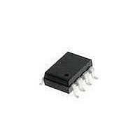
HCPL-263N-320E Avago Technologies US Inc., HCPL-263N-320E Datasheet - Page 17

HCPL-263N-320E
Manufacturer Part Number
HCPL-263N-320E
Description
OPTOCOUPLER 2CH 10MBD UL 8SMD GW
Manufacturer
Avago Technologies US Inc.
Datasheet
1.HCPL-061A-000E.pdf
(17 pages)
Specifications of HCPL-263N-320E
Package / Case
8-SMD Gull Wing
Voltage - Isolation
5000Vrms
Number Of Channels
2, Unidirectional
Current - Output / Channel
50mA
Data Rate
10MBd
Propagation Delay High - Low @ If
53ns @ 3.5mA
Current - Dc Forward (if)
10mA
Input Type
DC
Output Type
Open Collector
Mounting Type
Surface Mount, Gull Wing
Isolation Voltage
3750 Vrms
Maximum Continuous Output Current
50 mA
Maximum Fall Time
12 ns
Maximum Forward Diode Current
10 mA
Maximum Rise Time
42 ns
Minimum Forward Diode Voltage
1 V
Output Device
Logic Gate Photo IC
Configuration
2 Channel
Maximum Baud Rate
10 MBps
Maximum Forward Diode Voltage
1.6 V
Maximum Reverse Diode Voltage
3 V
Maximum Power Dissipation
60 mW
Maximum Operating Temperature
+ 85 C
Minimum Operating Temperature
- 40 C
Lead Free Status / RoHS Status
Lead free / RoHS Compliant
Available stocks
Company
Part Number
Manufacturer
Quantity
Price
Company:
Part Number:
HCPL-263N-320E
Manufacturer:
AVAGO
Quantity:
8 000
V
V
Figure 26. Parallel data transmission example.
The figure shows data and clock signals at the inputs and
outputs of the optocouplers. To obtain the maximum
data transmission rate, both edges of the clock signal are
being used to clock the data; if only one edge were used,
the clock signal would need to be twice as fast.
Propagation delay skew represents the uncertainty of
where an edge might be after being sent through an op-
tocoupler. Figure 26 shows that there will be uncertainty
in both the data and the clock lines. It is important that
these two areas of uncertainty not overlap, otherwise
the clock signal might arrive before all of the data out-
puts have settled, or some of the data outputs may start
I
I
Figure 25. Illustration of propagation delay skew – t
OUTPUTS
For product information and a complete list of distributors, please go to our website:
Avago, Avago Technologies, and the A logo are trademarks of Avago Technologies Limited in the United States and other countries.
Data subject to change. Copyright © 2007 Avago Technologies Limited. All rights reserved. Obsoletes AV01-0561EN
AV02-0391 - December 6, 2007
F
F
O
O
INPUTS
CLOCK
CLOCK
DATA
DATA
50%
50%
HCPL-261A fig 24
1.5 V
t
PSK
HCPL-2602 fig 17
t
PSK
t
PSK
1.5 V
TPHL
TPLH
PSK
.
www.avagotech.com
to change before the clock signal has arrived. From these
considerations, the absolute minimum pulse width that
can be sent through optocouplers in a parallel applica-
tion is twice t
longer pulse width to ensure that any additional uncer-
tainty in the rest of the circuit does not cause a prob-
lem.
The t
guaranteed specifications for propagation delays, pulse-
width distortion, and propagation delay skew over the
recommended temperature, input current, and power
supply ranges.
PSK
specified optocouplers offer the advantages of
PSK
. A cautious design should use a slightly


