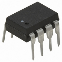
HCPL-4100-000E Avago Technologies US Inc., HCPL-4100-000E Datasheet - Page 7

HCPL-4100-000E
Manufacturer Part Number
HCPL-4100-000E
Description
OPTOCOUPLER TRANSMITTR 20MA 8DIP
Manufacturer
Avago Technologies US Inc.
Type
Transmitterr
Datasheet
1.HCPL-4100-000E.pdf
(12 pages)
Specifications of HCPL-4100-000E
Package / Case
8-DIP (0.300", 7.62mm)
Voltage - Isolation
3750Vrms
Input Type
DC
Voltage - Supply
4.5 V ~ 20 V
Operating Temperature
0°C ~ 70°C
Mounting Type
Through Hole
Logic Gate Type
Inverter
Maximum Baud Rate
0.02 MBd
Configuration
1 Channel
Isolation Voltage
3750 Vrms
Output Type
Open Collector
Maximum Propagation Delay Time
1600 ns
Maximum Forward Diode Current
7 mA
Maximum Continuous Output Current
30 mA
Maximum Power Dissipation
360 mW
Maximum Operating Temperature
+ 70 C
Minimum Operating Temperature
0 C
No. Of Channels
1
Optocoupler Output Type
Transistor
Input Current
250µA
Output Voltage
27V
Opto Case Style
DIP
No. Of Pins
8
Data Rate Max
24Kbps
Rohs Compliant
Yes
Lead Free Status / RoHS Status
Lead free / RoHS Compliant
Lead Free Status / RoHS Status
Lead free / RoHS Compliant, Lead free / RoHS Compliant
Other names
516-1546-5
Available stocks
Company
Part Number
Manufacturer
Quantity
Price
Company:
Part Number:
HCPL-4100-000E
Manufacturer:
AVAGO
Quantity:
5 000
Part Number:
HCPL-4100-000E
Manufacturer:
AVAGO/安华高
Quantity:
20 000
Notes:
10. Common mode transient immunity in the logic high level is the maximum (positive) dV
11. Common mode transient immunity in the logic low level is the maximum (positive) dV
12. Use of a 0.1 μF bypass capacitor connected between pins 5 and 8 is recommended.
13. In accordance with UL 1577, each optocoupler is momentary withstand proof tested by applying an insulation test voltage ≥ 4500 V rms for 1
Figure 3. Typical Mark State Output Voltage vs.
Temperature.
7
1. Derate linearly above 55°C free air temperature at a rate of 3.8 mW/ °C. Proper application of the derating factors will prevent IC junction
2. Derate linearly above a free-air temperature of 70°C at a rate of 2.3 mW/ °C. A significant amount of power may be dissipated in the HCPL-4100
3. Derate linearly above 55°C free-air temperature at a rate of 5.1 mW/ °C.
4. The maximum current that will flow into the output in the mark state (I
5. The device is considered a two terminal device, pins 1, 2, 3, and 4 are connected together, and pins 5, 6, 7, and 8 are connected together.
6. The t
7. The t
8. The rise time, t
9. The fall time, t
temperatures from exceeding 125°C for ambient temperatures up to 85°C.
output circuit during the transition from the SPACE state to the MARK state when driving a data line or capacitive load (C
dissipation during the transition can be estimated from the following equation which assumes a linear discharge of a capacitive load: P = I
+ V
applications driving twisted pair data lines with NRZ data as shown in Figure 12, the transition time will be less than 10% of one bit time.
short circuit shall not exceed 10 ms.
the output pulse.
the output pulse.
V
V
second (leakage detection current limit, I
3.0
2.8
2.6
2.4
2.2
2.0
1.8
1.6
1.4
1.2
CM
CM
, that can be sustained with the output in a Space (“L”) state (i.e., I
MO
, that can be sustained with the output in a Mark (“H”) state (i.e., I
PLH
PHL
-40
)/2, where V
propagation delay is measured from the 1.3 volt level on the leading edge of the input pulse to the 10 mA level on the leading edge of
propagation delay is measured from the 1.3 volt level on the trailing edge of the input pulse to the 10 mA level on the trailing edge of
20 mA
12 mA
2 mA
-20
I
O
T
A
f
– TEMPERATURE – °C
, is measured from the 90% to the 10% level on the falling edge of the output current pulse.
r
, is measured from the 10% to the 90% level on the rising edge of the output current pulse.
0
SO
is the output voltage in the SPACE state. The duration of this transition can be estimated as t = C
20
40
V
60
V
CC
I
= 2 V
= 5 V
80
100
i-o
≤ 5 μA).
Figure 4. Typical Output Voltage vs. Loop Cur-
rent.
3.5
3.0
2.5
2.0
1.5
1.0
0.5
0
0
5
I
O
– OUTPUT CURRENT – mA
10
O
O
> 12 mA).
< 3 mA).
SC
15
) is internally limited to protect the device. The duration of the output
V
V
T
A
CC
I
= 2 V
= 25 °C
20
= 5 V
25
CM
CM
/dt on the leading edge of the common mode pulse,
30
/dt on the leading edge of the common mode pulse,
Figure 5. Typical Space State Output Current vs.
Temperature.
1.0
1.3
1.2
1.1
0.9
0.8
0.7
0.6
-40
27 V
20 V
V
-20
O
T
A
– TEMPERATURE – °C
OUT
0
(V
OUT
20
SO
). The average power
- V
MO
40
)/I
V
V
SC
60
CC
I
. For typical
= 0.8 V
= 5 V
80
SC
(V
100
SO


