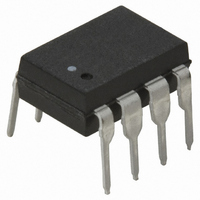
HCPL-2602-000E Avago Technologies US Inc., HCPL-2602-000E Datasheet - Page 6

HCPL-2602-000E
Manufacturer Part Number
HCPL-2602-000E
Description
OPTOCOUPLER LOG-OUT 1CHAN 8-DIP
Manufacturer
Avago Technologies US Inc.
Type
Line Receiverr
Datasheet
1.HCPL-2612-000E.pdf
(16 pages)
Specifications of HCPL-2602-000E
Package / Case
8-DIP (0.300", 7.62mm)
Voltage - Isolation
3750Vrms
Input Type
AC, DC
Voltage - Supply
4.5 V ~ 5.5 V
Operating Temperature
0°C ~ 70°C
Mounting Type
Through Hole
Isolation Voltage
3750 Vrms
Maximum Continuous Output Current
50 mA
Maximum Fall Time
0.01 us
Maximum Forward Diode Current
60 mA
Output Device
Integrated Photo IC
Configuration
1 Channel
Maximum Baud Rate
10 MBd
Maximum Forward Diode Voltage
2.7 V
Maximum Reverse Diode Voltage
0.95 V
Maximum Power Dissipation
40 mW
Maximum Operating Temperature
+ 70 C
Minimum Operating Temperature
0 C
Number Of Elements
1
Output Type
Open Collector
Baud Rate
10Mbps
Forward Voltage
2.7V
Forward Current
60mA
Output Current
50mA
Package Type
PDIP
Operating Temp Range
0C to 70C
Power Dissipation
40mW
Propagation Delay Time
75ns
Pin Count
8
Mounting
Through Hole
Reverse Breakdown Voltage
0.95V
Operating Temperature Classification
Commercial
No. Of Channels
1
Optocoupler Output Type
Logic Gate
Input Current
60mA
Output Voltage
5.5V
Opto Case Style
DIP
No. Of Pins
8
Input Current Max
60mA
Rohs Compliant
Yes
Lead Free Status / RoHS Status
Lead free / RoHS Compliant
Lead Free Status / RoHS Status
Lead free / RoHS Compliant, Lead free / RoHS Compliant
Other names
516-1662-5
Available stocks
Company
Part Number
Manufacturer
Quantity
Price
Company:
Part Number:
HCPL-2602-000E
Manufacturer:
AVAGO
Quantity:
30 000
Absolute Maximum Ratings (No Derating Required up to 85 C)
6
Recommended Operating Conditions
*The initial switching threshold is 5 mA or less. It is recommended that an input current between
6.3 mA and 10 mA be used to obtain best performance and to provide at least 20% LED degradation
guardband.
Parameter
Input Current, Low Level
Input Current, High Level
Supply Voltage, Output
High Level Enable Voltage
Low Level Enable Voltage
Fan Out (@ R
Output Pull-up Resistor
Operating Temperature
Parameter
Storage Temperature
Operating Temperature
Forward Input Current
Reverse Input Current
Input Current, Pin 4
Supply Voltage (1 Minute Maximum)
Enable Input Voltage (Not to Exceed V
more than 500 mV)
Output Collector Current
Output Collector Voltage (Selection for Higher
Output Voltages up to 20 V is Available.)
Output Collector Power Dissipation
Lead Solder Temperature
Solder Reflow Temperature Profile
L
= 1 k )
Symbol
V
V
V
R
CC
I
I
T
N
IH
CC
EH
IL
EL
A
L
by
Min.
330
4.5
2.0
5*
0
0
0
Max.
250
V
4 K
5.5
0.8
60
70
5
CC
Symbol
V
T
P
T
T
I
V
V
I
I
IR
CC
LS
O
A
O
S
I
E
O
TTL Loads
Units
mA
V
V
V
A
C
See Package Outline Drawings section
Min.
-55
-40
-10
260 C for 10 sec., 1.6 mm below
seating plane
V
CC
Max.
125
85
60
60
10
50
40
7
7
+ 0.5
Units
mW
mA
mA
mA
mA
V
V
V
C
C


