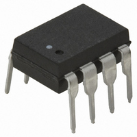
HCPL-2602 Avago Technologies US Inc., HCPL-2602 Datasheet

HCPL-2602
Specifications of HCPL-2602
Available stocks
Related parts for HCPL-2602
HCPL-2602 Summary of contents
Page 1
... CAUTION advised that normal static precautions be taken in handling and assembly of this component to prevent damage and/or degradation which may be induced by ESD. Features • 1000 V/ s minimum Common Mode Rejection (CMR for HCPL-2602 and 3.5 kV/ s minimum CM CMR at V • Line termination included – no extra circuitry required • Accepts a broad range of drive conditions • ...
Page 2
... The HCPL-2602/12 are useful as line receivers in high noise environments that conventional line receivers cannot tolerate. The higher LED threshold voltage provides improved immunity to differential noise and the internally shielded detector provides orders of magnitude improvement in common mode rejection with little or no sacrifice in speed. ...
Page 3
... To order, choose a part number from the part number column and combine with the desired option from the option column to form an order entry. Example 1: HCPL-2602-500E to order product of Gull Wing Surface Mount package in Tape and Reel packaging and RoHS compliant. Example 2: HCPL-2612 to order product of 300 mil DIP package in Tube packaging and non RoHS compliant. ...
Page 4
Package Outline Drawings 8-Pin DIP Package 9.65 ± 0.25 (0.380 ± 0.010 XXXXZ YYWW 1 2 1.19 (0.047) MAX. 3.56 ± 0.13 (0.140 ± 0.005) 1.080 ± 0.320 (0.043 ± 0.013) 8-Pin DIP Package with Gull Wing ...
Page 5
... V DIN IEC 112/VDE 0303 Part 1 IIIa Material Group (DIN VDE 0110, 1/89, Table 1) Regulatory Information The HCPL-2602/2612 have been approved by the following organizations: UL Recognized under UL 1577, Component Recognition Program, File E55361. CSA ...
Page 6
Absolute Maximum Ratings (No Derating Required Parameter Storage Temperature Operating Temperature Forward Input Current Reverse Input Current Input Current, Pin 4 Supply Voltage (1 Minute Maximum) Enable Input Voltage (Not to Exceed V more than 500 ...
Page 7
Electrical Characteristics Over recommended temperature (T A Parameter Sym. High Level Output I OH Current Low Level Output V OL Voltage High Level Supply I CCH Current Low Level Supply I CCL Current High Level Enable I EH Current Low ...
Page 8
... ELH Time of Enable from Propagation Delay t EHL Time of Enable from Common Mode HCPL-2602 Transient | Immunity at High HCPL-2612 Output Level Common Mode HCPL-2602 Transient | Immunity at Low HCPL-2612 Output Level *All typicals Package Characteristics All Typicals Parameter Sym. Input-Output Momentary V ISO * Withstand Voltage ...
Page 9
Notes: 1. Bypassing of the power supply line is required, with a 0.1 F ceramic disc capacitor adjacent to each optocoupler as illustrated in Figure 15. Total lead length between both ends of the capacitor and the isolator pins should ...
Page 10
I I PULSE GEN INPUT 3 MONITORING NODE GND *C IS APPROXIMATELY 15 pF WHICH INCLUDES L PROBE AND STRAY WIRING CAPACITANCE. ...
Page 11
RISE FALL 300 L 290 350 350 ...
Page 12
... C 16t where peaking capacitance in picofarads t = data bit interval in nanoseconds Polarity Reversing Drive A single HCPL-2602/12 can also be used with polarity reversing drive (Figure b). Current reversal is obtained by way of the substrate isolation diode (substrate to collector). Some reduction of data rate occurs, however, because the substrate ...
Page 13
Figure a. Polarity non-reversing. Figure b. Polarity reversing, single ended. Figure c. Polarity reversing, split phase. Figure d. Flip-flop configurations. ...
Page 14
... Line drivers designed for RS-422 and RS-423 generally provide adequate voltage and current for operating the HCPL-2602/12. Most drivers also have characteristics allowing the HCPL-2602/ connected directly to the driver terminals. Worst case drive conditions, however, would require current shunting to prevent overstress of the HCPL- 2602/12 ...
Page 15
I I 50 PSK Figure 16. Illustration of propagation delay skew - t 15 DATA INPUTS CLOCK DATA OUTPUTS CLOCK Figure 17. Parallel data transmission example. . PSK ...
Page 16
For product information and a complete list of distributors, please go to our website: Avago, Avago Technologies, and the A logo are trademarks of Avago Technologies Limited in the United States and other countries. Data subject to change. Copyright © ...


