PC817XJ0000F Sharp Microelectronics, PC817XJ0000F Datasheet
PC817XJ0000F
Specifications of PC817XJ0000F


Related parts for PC817XJ0000F


PC817XJ0000F Summary of contents
Page 1
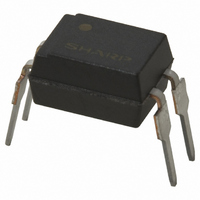
... Series ∗ 4-channel package type is also available. (model No. PC847XJ0000F Series) ■ Description PC817XJ0000F Series contains an IRED optically coupled to a phototransistor packaged in a 4pin DIP, available in wide-lead spacing option and SMT gullwing lead-form option. Input-output isolation voltage(rms) is 5.0kV. Collector-emitter voltage is 80V and CTR is 50% to 600% at input current of 5mA. ■ ...
Page 2
... Internal Connection Diagram 1 2 ■ Outline Dimensions 1. Through-Hole [ex. PC817XJ0000F] Rank mark Anode mark Factory identification mark Date code C817 2 3 ±0.5 6.5 ±0.3 7.62 Epoxy resin ±0.1 0.26 θ θ θ 13˚ Product mass : approx. 0.23g 3. Wide Through-Hole Lead-Form [ex. PC817XFJ000F] ...
Page 3
... Rank mark Refer to the Model Line-up table 2nd digit Month of production Month Mark January 1 February 2 March 3 April 4 May 5 June 6 July 7 August 8 September 9 October O November N December D Plating material Japan SnCu (Cu : TYP. 2%) Indonesia SnBi (Bi : TYP. 2%) China SnCu (Cu : TYP. 2%)* 3 PC817XJ0000F Series Sheet No.: D2-A03102EN ...
Page 4
... F I =5mA =20mA, I =1mA F C DC500V 60%RH V=0, f=1MHz V =5V, I =2mA, R =100Ω, −3dB =2V, I =2mA, R =100Ω PC817XJ0000F Series (T =25˚C) a MIN. TYP. MAX. Unit − 1.2 1.4 V − − 3.0 V − − 10 µA − 30 250 pF − − 100 nA 80 − ...
Page 5
... PC817XFPJ00F A − B − C − − D − − − − − − PC817XJ0000F Series I [mA =5mA, V =5V, T =25˚ 2.5 to 30.0 4.0 to 8.0 6.5 to 13.0 10.0 to 20.0 15.0 to 30.0 4.0 to 13.0 6.5 to 20.0 10.0 to 30.0 4.0 to 20.0 6.5 to 30.0 4.0 to 30.0 I ...
Page 6
... Ambient Temperature 75 100 125 (˚C) a Fig.4 Total Power Dissipation vs. Ambient Temperature 75 100 125 (˚C) a Fig.6 Current Transfer Ratio vs. Forward Current 500 =25˚C a 400 300 200 100 − PC817XJ0000F Series 100 − 100 Ambient temperature T (˚C) a 250 200 150 100 50 0 − ...
Page 7
... F Fig.10 Collector - emitter Saturation Voltage vs. Ambient Temperature 0.14 =5V 0.12 =5mA,V = 0.08 0.06 0.04 0. 100 (˚C) a Fig.12 Collector-emitter Saturation Voltage vs. Forward Current V =50V 100 (˚ PC817XJ0000F Series 30 I =30mA T =25˚ 20mA P (MAX 10mA 10 5mA Collector-emitter voltage V ( =20mA F I ...
Page 8
... Fig.14 Test Circuit for Response Time t r Input Please refer to the conditions in Fig.13. 10 (kΩ) L Fig.16 Test Circuit for Frequency Response V = =2mA C T =25˚C a 100Ω 1kΩ 100 8 PC817XJ0000F Series Input V CC Output R Output Output Please refer to the conditions in Fig.15. Sheet No.: D2-A03102EN ...
Page 9
... In the case of long term operation, please take the general IRED degradation (50% degradation over 5 years) into the design consideration. ● Recommended Foot Print (reference) SMT Gullwing Lead-form 8.2 2.2 ✩ For additional design assistance, please review our corresponding Optoelectronic Application Notes. PC817XJ0000F Series Wide SMT Gullwing Lead-form 10.2 2.2 9 (Unit : mm) Sheet No.: D2-A03102EN ...
Page 10
... Please test the soldering method in actual condition and make sure the soldering works fine, since the impact on the junction between the device and PCB varies depending on the tooling and soldering conditions. Reflow 220˚C or more, 60s or less PC817XJ0000F Series 4 (min) Sheet No.: D2-A03102EN ...
Page 11
... Specific brominated flame retardants such as the PBBOs and PBBs are not used in this product at all. This product shall not contain the following materials banned in the RoHS Directive (2002/95/EC). •Lead, Mercury, Cadmium, Hexavalent chromium, Polybrominated biphenyls (PBB), Polybrominated di- phenyl ethers (PBDE). PC817XJ0000F Series 11 Sheet No.: D2-A03102EN ...
Page 12
... MAX. 100pcs of products shall be packaged in a sleeve. Both ends shall be closed by tabbed and tabless stoppers. The product shall be arranged in the sleeve with its anode mark on the tabless stopper side. MAX. 20 sleeves in one case. Sleeve outline dimensions 15.0 6.35 PC817XJ0000F Series 12 (Unit : mm) (Unit : mm) Sheet No.: D2-A03102EN ...
Page 13
... Direction of product insertion ±0.1 ±0.1 ±0.1 ±0.1 1.75 8.0 2 ±0.05 ±0.1 ±0.1 4.2 5.1 Dimensions List f b Pull-out direction 13 PC817XJ0000F Series J I (Unit : mm ±0.1 +0.1 4.0 φ1.5 −0 (Unit : mm ±1.5 ±1.0 ±0.5 330 17.5 100 ±1.0 ±0.5 ±0.5 23 2.0 2.0 [Packing : 2 000pcs/reel] Sheet No ...
Page 14
... Direction of product insertion ±0.1 ±0.1 ±0.1 ±0.1 1.75 8.0 2 ±0.05 ±0.1 ±0.1 4.1 5.1 Dimensions List f b Pull-out direction 14 PC817XJ0000F Series J I (Unit : mm ±0.1 +0.1 4.0 φ1.5 −0 (Unit : mm ±1.5 ±1.0 ±0.5 330 25.5 100 ±1.0 ±0.5 ±0.5 23 2.0 2.0 [Packing : 2 000pcs/reel] ...
Page 15
... Measures such as fail-safe function and redundant design should be taken to ensure reliability and safety when SHARP devices are used for or in connection [E178] PC817XJ0000F Series with equipment that requires higher reliability such as: --- Transportation control and safety equipment (i.e., aircraft, trains, automobiles, etc.) ...