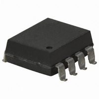
HCNW4562-300E Avago Technologies US Inc., HCNW4562-300E Datasheet

HCNW4562-300E
Specifications of HCNW4562-300E
Related parts for HCNW4562-300E
HCNW4562-300E Summary of contents
Page 1
... HCPL-4562, HCNW4562 High Bandwidth, Analog/Video Optocouplers Data Sheet Description The HCPL-4562 and HCNW4562 optocouplers provide wide bandwidth isolation for analog signals. They are ideal for video isolation when combined with their application circuit (Figure 4). High linearity and low phase shift are achieved through an AlGaAs LED combined with a high speed detector ...
Page 2
... Selection Guide Single Channel Packages 8-Pin DIP (300 Mil) HCPL-4562 Ordering Information HCPL-4562 is UL Recognized with 3750 Vrms for 1 minute per UL1577 unless otherwise specified. HCNW4562 is UL Recognized with 5000 Vrms for 1 minute per UL1577. Option Part RoHS non RoHS Number ...
Page 3
Package Outline Drawings 8-Pin DIP Package (HCPL-4562) 9.65 ± 0.25 (0.380 ± 0.010 TYPE NUMBER A XXXXZ R YYWW 1.19 (0.047) MAX. 3.56 ± 0.13 (0.140 ± 0.005) 1.080 ± 0.320 (0.043 ± 0.013) ...
Page 4
... A HCNWXXXX YYWW 2.54 (0.100) TYP. 1.78 ± 0.15 (0.070 ± 0.006) 8-Pin Widebody DIP Package with Gull Wing Surface Mount Option 300 (HCNW4562) 11.15 ± 0.15 (0.442 ± 0.006 1.78 ± 0.15 (0.070 ± 0.006) 2.54 (0.100) BSC DIMENSIONS IN MILLIMETERS (INCHES) ...
Page 5
... TIME (SECONDS) TIME WITHIN 5 °C of ACTUAL PEAK TEMPERATURE t p 20-40 SEC. RAMP-DOWN 6 °C/SEC. MAX 150 SEC. IEC/EN/DIN EN 60747-5-2 Approved under: IEC 60747-5-2:1997 + A1:2002 EN 60747-5-2:2001 + A1:2002 DIN EN 60747-5-2 (VDE 0884 Teil 2):2003-01 (HCNW4562 only) PEAK TEMP. 230°C TIGHT TYPICAL LOOSE 250 ...
Page 6
... Tracking Index) Isolation Group Option 300 - surface mount classification is Class A in accordance with CECC 00802. IEC/EN/DIN EN 60747-5-2 Insulation Related Characteristics (HCNW4562 ONLY) Description Installation classification per DIN VDE 0110/1.89, Table 1 for rated mains voltage ≤ 600 V rms for rated mains voltage ≤ 1000 V rms Climatic Classification Pollution Degree (DIN VDE 0110/1 ...
Page 7
... F(avg) HCNW4562 I HCPL-4562 F(PEAK) HCNW4562 I HCPL-4562 F(EFF) V HCPL-4562 R HCNW4562 P HCNW4562 IN I O(AVG) I O(PEAK) V EBR HCPL-4562 LS HCNW4562 T Option RP 300 Symbol Device T HCPL-4562 A I HCPL-4562 FQ HCNW4562 I HCPL-4562 F(PEAK) HCNW4562 Min. Max. Units -55 125 °C -40 85 ° 18 12.9 mA rms 100 mW 260 °C 260 ° ...
Page 8
... Input Reverse BV HCPL-4562 R Breakdown HCNW4562 Voltage Transistor h FE Current Gain Current CTR HCPL-4562 Transfer Ratio HCNW4562 DC Output V HCPL-4562 OUT Voltage HCNW4562 for HCNW4562 (i.e., Recommended I F Min. Typ.* Max. Units µA 19.2 -0.3 %/°C 0.25 % 0.15 1.1 1.3 1.6 V 1.2 1.6 1.8 1 ...
Page 9
... Phase 3.58 MHz HCNW4562 Total Harmonic THD HCPL-4562 Distortion HCNW4562 Output Noise V (noise) O Voltage Isolation Mode IMRR HCPL-4562 Rejection Ratio HCNW4562 for HCNW4562 (i.e., Recommended I F Device Min. Typ.* Max. Units 0.8 2.0 4.2 3.0 -0.3 %/°C V 1.1 3.0 -dB 0. MHz ...
Page 10
... the forward LED input current )/(V /V )], where V is the isolation mode voltage signal. OUT IN OUT IM IM Units Test Conditions Fig. V rms RH ≤50 min 25°C A Ω 500 Vdc I 25° 100° MHz = 10 mA (HCNW4562). , times 100%. F Note ...
Page 11
... Figure 1. Gain and bandwidth test circuit Figure 2. Base photo current test circuit Figure 4. Recommended isolated video interface circuit 11 162 Ω (HCPL-4562) 90.9 Ω (HCNW4562) Figure 3. Base photo current frequency response test circuit ...
Page 12
... INPUT CURRENT – Figure 6. Base photo current vs. input current HCPL-4562 fig 6a HCPL-4562 1.02 1 PHASE 0.98 0.96 NORMALIZED GAIN 3.58 MHz 0. °C A SEE FIG – INPUT CURRENT – Figure 7. Small-signal response vs. input current HCPL-4562 fig 7a 12 HCNW4562 1.5 HCNW4562 HCNW4562 ...
Page 13
... Figure 9. Current transfer ratio vs. input current HCPL-4562 fig 9a HCPL-4562 -0.9 -1.1 FREQUENCY = 6 MHz -1.3 -1.5 -1.7 FREQUENCY = 10 MHz -1.9 -2 ° 0.1 MHz REF -2.5 -2 – QUIESCENT INPUT CURRENT – Figure 10. Base photo current variation vs. bias conditions HCPL-4562 fig 10a 13 HCNW4562 HCNW4562 HCNW4562 ...
Page 14
... Figure 12. Normalized base photo current vs. frequency HCPL-4562 fig 12a HCPL-4562 0 I PHASE PB -25 SEE FIGURE 3 -50 - °C A -100 -125 VIDEO INTERFACE -150 CIRCUIT PHASE -175 SEE FIGURE 4 -200 -225 -250 – FREQUENCY – MHz Figure 13. Phase vs. frequency HCPL-4562 fig 13a 14 HCNW4562 HCNW4562 HCNW4562 ...
Page 15
... ADDITIONAL Q 4 BUFFER STAGE OUT LOW IMPEDANCE LOAD Figure 16. Output buffer stage for low imped- ance loads 15 HCPL-4562 fig 16 HCNW4562 HCNW4562 HCNW4562 1000 P (mW) S 900 I (mA) S 800 700 600 500 400 300 200 100 100 125 150 175 T – CASE TEMPERATURE – °C S Figure 17 ...
Page 16
... Conversion from HCPL-4562 to HCNW4562 In order to obtain similar circuit performance when converting from the HCPL-4562 to the HCNW4562 recommended to increase the Quiescent Input Current from mA. If the application circuit FQ in Figure 4 is used, then potentiometer R4 should be adjusted appropriately. Design Considerations of the Application Circuit The appÏ ...
Page 17
For product information and a complete list of distributors, please go to our website: Avago, Avago Technologies, and the A logo are trademarks of Avago Technologies Limited in the United States and other countries. Data subject to change. Copyright © ...


