MT18VDDF12872Y-40BF1 Micron Technology Inc, MT18VDDF12872Y-40BF1 Datasheet
MT18VDDF12872Y-40BF1
Specifications of MT18VDDF12872Y-40BF1
MT18VDDF12872Y-40BF1


Related parts for MT18VDDF12872Y-40BF1


MT18VDDF12872Y-40BF1 Summary of contents
Page 1
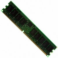
... ECC, SR) PC3200 184-PIN DDR SDRAM RDIMM MT18VDDF6472 – 512MB MT18VDDF12872 – 1GB For the latest data sheet, please refer to the Micron site: www.micron.com/products/modules Figure 1: 184-Pin DIMM (MO-206) Low-Profile 1.125in. (28.58mm) Very Low Profile 0.72in. (18.29mm) OPTIONS • Operating Temperature Range Commercial (0° ...
Page 2
... DENSITY MT18VDDF6472G-40B__ 512MB MT18VDDF6472Y-40B__ 512MB MT18VDDF12872G-40B__ MT18VDDF12872Y-40B__ NOTE: All part numbers end with a two-place code (not shown), designating component and PCB revisions. Consult factory for current revision codes. Example: MT18VDDF6472G-40BB1. pdf: 09005aef80f6b913, source: 09005aef80f6b41c DDAF18C64_128x72G.fm - Rev. C 9/04 EN 512MB, 1GB (x72, ECC, SR) PC3200 ...
Page 3
Table 3: Pin Assignment (184-Pin DIMM Front) PIN SYMBOL PIN SYMBOL PIN SYMBOL PIN SYMBOL DQ17 47 REF 2 DQ0 25 DQS2 DQ1 DQS0 ...
Page 4
Table 5: Pin Descriptions Pin numbers may not correlate with symbol; refer to Pin Assignment Tables for pin number and symbol information. PIN NUMBERS SYMBOL 10 RESET# 63, 65, 154 WE#, CAS#, RAS# 137, 138 CK0, CK0# 21 157 52, ...
Page 5
Table 5: Pin Descriptions Pin numbers may not correlate with symbol; refer to Pin Assignment Tables for pin number and symbol information. PIN NUMBERS SYMBOL 12,13, 19, 20, DQ0–DQ63 23, 24, 28, 31, 33, 35, 39, ...
Page 6
... SERIAL PD R SCL U12 SA0 SA1 SA2 RESET# Standard modules use the following DDR SDRAM devices: MT46V64M4FG (512MB); MT46V128M4FG (1GB) Lead-free modules use the following DDR SDRAM devices: MT46V64M4BG (512MB); MT46V128M4BG (1GB) 6 184-PIN DDR SDRAM RDIMM DQS CS U24 DQS CS U23 DQS CS# DM ...
Page 7
... RESET# SA0 SA1 SA2 Standard modules use the following DDR SDRAM devices: MT46V64M4FG (512MB); MT46V128M4FG (1GB) Lead-free modules use the following DDR SDRAM devices: MT46V64M4BG (512MB); MT46V128M4BG (1GB) Micron Technology, Inc., reserves the right to change products or specifications without notice. 7 DQS CS U22 ...
Page 8
... DDR SDRAM modules use internally configured quad-bank DDR SDRAM devices. DDR SDRAM modules use a double data rate archi- tecture to achieve high-speed operation. The double data rate architecture is essentially a 2n-prefetch architecture with an interface designed to transfer two data words per clock cycle at the I/O pins ...
Page 9
Vio- lating either of these requirements will result in unspecified operation. Mode register bits A0–A2 specify the burst length, A3 specifies the type of burst (sequential or inter- leaved), A4–A6 specify the CAS latency, ...
Page 10
Table 6: Burst Definition Table ORDER OF ACCESSES WITHIN STARTING BURST COLUMN TYPE = LENGTH ADDRESS SEQUENTIAL 0 0-1-2 1-2-3 2-3-0 3-0-1 ...
Page 11
A8 set to one, and bits A0–A6 set to the desired values. Although not required by the Micron device, JEDEC specifications recommend when a LOAD MODE REGISTER command is issued to reset the DLL, it should always ...
Page 12
Commands Table 8, Commands Truth Table, and Table 9, DM Operation Truth Table, provide a general reference of available commands. For a more detailed description Table 8: Commands Truth Table CKE is HIGH for all commands shown except SELF REFRESH; ...
Page 13
Absolute Maximum Ratings Stresses greater than those listed may cause perma- nent damage to the device. This is a stress rating only, and functional operation of the device at these or any other conditions above those indicated in the opera- ...
Page 14
Table 11: IDD Specifications and Conditions – 512MB DDR SDRAM components only Notes: 1–5, 8, 10, 12, 48; notes appear on pages 18–20; 0°C PARAMETER/CONDITION OPERATING CURRENT: One device bank; Active-Precharge (MIN); DQ, DM and ...
Page 15
Table 12: IDD Specifications and Conditions – 1GB DDR SDRAM components only Notes: 1–5, 8, 10, 12, 48; notes appear on pages 18–20; 0°C PARAMETER/CONDITION OPERATING CURRENT: One device bank; Active-Precharge (MIN (MIN); DQ, DM ...
Page 16
Table 13: Capacitance Note: 11; notes appear on pages 18–20 PARAMETER Input/Output Capacitance: DQ, DQS Input Capacitance: Command and Address, S#, CKE Input Capacitance: CK, CK# Table 14: DDR SDRAM Component Electrical Characteristics and Recommended AC Operating Conditions Notes: 1–5, ...
Page 17
Table 14: DDR SDRAM Component Electrical Characteristics and Recommended AC Operating Conditions (Continued) Notes: 1–5, 12-15, 29; notes appear on pages 18–20; 0°C AC CHARACTERISTICS PARAMETER ACTIVE to READ or WRITE delay PRECHARGE command period DQS read preamble DQS read ...
Page 18
Notes 1. All voltages referenced Tests for AC timing and electrical AC and DC DD characteristics may be conducted at nominal ref- erence/supply voltage levels, but the related spec- ifications and device operation are ...
Page 19
DRAM controller greater than eight refresh cycles is not allowed. 22. The valid data window is derived by achieving t t other specifications CK/2 QHS). The data valid window ...
Page 20
The voltage levels used are derived from a mini- mum V level and the referenced test load practice, the voltage levels obtained from a prop- erly terminated bus will provide significantly dif- ferent voltage values. 35. V ...
Page 21
Initialization To ensure device operation the DRAM must be ini- tialized as described below: 1. Simultaneously apply power Apply V and then V power. REF TT 3. Assert and hold CKE at a LVCMOS logic low. 4. ...
Page 22
Table 15: PLL Clock Driver Timing Requirements and Switching Characteristics Note: 1 PARAMETER SYMBOL Operating Clock Frequency Input Duty Cycle Stabilization Time Cycle to Cycle Jitter Static Phase Offset Output Clock Skew Period Jitter Half-Period Jitter t Input Clock Slew ...
Page 23
Table 16: Register Timing Requirements and Switching Characteristics Note: 1 REGISTER SYMBOL PARAMERTER f Clock Frequency clock t Clock to Output Time pd t Reset to Output Time PHL t Pulse Duration w SSTL (bit pattern t Differential Inputs Active ...
Page 24
... NOTE: 1. Micron Technology, Inc. recommends a minimum air flow of 1 meter/second (~197 LFM) across all modules. 2. The component case temperature measurements shown above were obtained experimentally. The typical system to be used for experimental purposes is a dual-processor 600 MHz work station, fully loaded, with four comparable registered memory modules ...
Page 25
SPD Clock and Data Conventions Data states on the SDA line can change only during SCL LOW. SDA state changes during SCL HIGH are reserved for indicating start and stop conditions (as shown in Figure 12, Data Validity, and Figure ...
Page 26
Table 17: EEPROM Device Select Code The most significant bit (b7) is sent first SELECT CODE Memory Area Select Code (two arrays) Protection Register Select Code Table 18: EEPROM Operating Modes MODE RW BIT Current Address Read Random Address Read ...
Page 27
Table 19: Serial Presence-Detect EEPROM DC Operating Conditions All voltages referenced DDSPD PARAMETER/CONDITION SUPPLY VOLTAGE INPUT HIGH VOLTAGE: Logic 1; All inputs INPUT LOW VOLTAGE: Logic 0; All inputs OUTPUT LOW VOLTAGE 3mA ...
Page 28
Table 21: Serial Presence-Detect Matrix “1”/“0”: Serial Data, “driven to HIGH”/“driven to LOW”; notes at end of Serial Presence-Detect Matrix BYTE DESCRIPTION 0 Number of SPD Bytes Used by Micron 1 Total Number of Bytes In SPD Device 2 Fundamental ...
Page 29
Table 21: Serial Presence-Detect Matrix “1”/“0”: Serial Data, “driven to HIGH”/“driven to LOW”; notes at end of Serial Presence-Detect Matrix BYTE DESCRIPTION 45 SDRAM Device Max Read Data Hold Skew Factor t ( QHS) 46-61 Reserved 47 DIMM Height 48-61 ...
Page 30
Figure 16: 184-Pin DIMM Dimensions – Low-Profile PCB 0.079 (2.00) R (4X 0.098 (2.50) D (2X) 0.091 (2.30) TYP. PIN 1 0.050 (1.27) TYP. 0.091 (2.30) TYP. U15 U16 U17 PIN 184 Figure 17: 184-Pin DIMM Dimensions ...
Page 31
Data Sheet Designation Released (No Mark): This data sheet contains mini- mum and maximum limits specified over the complete power supply and temperature range for production 8000 S. Federal Way, P.O. Box 6, Boise, ID 83707-0006, Tel: 208-368-3900 E-mail: prodmktg@micron.com, ...