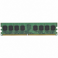
HYS64T128020HU-3S-B Qimonda, HYS64T128020HU-3S-B Datasheet - Page 35

HYS64T128020HU-3S-B
Manufacturer Part Number
HYS64T128020HU-3S-B
Description
MODULE DDR2 1GB 240-DIMM
Manufacturer
Qimonda
Datasheet
1.HYS64T64000HU-3S-B.pdf
(87 pages)
Specifications of HYS64T128020HU-3S-B
Memory Type
DDR2 SDRAM
Memory Size
1GB
Speed
333MHz
Package / Case
240-DIMM
Lead Free Status / RoHS Status
Lead free / RoHS Compliant
Other names
675-1024
3.4
List of tables defining
•
•
•
•
•
•
•
•
Rev. 1.3, 2006-12
03292006-6GMD-RSFT
Parameter
Operating Current 0
One bank Active - Precharge;
valid commands. Address and control inputs are SWITCHING, Databus inputs are SWITCHING.
Operating Current 1
One bank Active - Read - Precharge;
t
control inputs are SWITCHING, Databus inputs are SWITCHING.
Precharge Standby Current
All banks idle; CS is HIGH; CKE is HIGH;
Databus inputs are SWITCHING.
Precharge Power-Down Current
Other control and address inputs are STABLE, Data bus inputs are FLOATING.
Precharge Quiet Standby Current
All banks idle; CS is HIGH; CKE is HIGH;
Data bus inputs are FLOATING.
Active Standby Current
Burst Read: All banks open; Continuous burst reads; BL = 4; AL = 0, CL = CL
t
SWITCHING; Data Bus inputs are SWITCHING;
Active Power-Down Current
All banks open;
are FLOATING. MRS A12 bit is set to LOW (Fast Power-down Exit);
Active Power-Down Current
All banks open; t
are FLOATING. MRS A12 bit is set to HIGH (Slow Power-down Exit);
Operating Current - Burst Read
All banks open; Continuous burst reads; BL = 4; AL = 0, CL = CL
t
bus inputs are SWITCHING;
Operating Current - Burst Write
All banks open; Continuous burst writes; BL = 4; AL = 0, CL = CL
t
SWITCHING; Data Bus inputs are SWITCHING;
RCD
RAS
RP
RAS
Table 22 “IDD Measurement Conditions” on Page 35
Table 23 “Definitions for IDD” on Page 36
Table 25 “IDD Specification for HYS[64/72]T[32/64/128]0x0HU-2.5-B” on Page 38
Table 26 “IDD Specification for HYS[64/72]T[32/64/128]0x0HU-3-B” on Page 39
Table 27 “IDD Specification for HYS[64/72]T[32/64/128]xx0HU-3S-B” on Page 40
Table 27 “IDD Specification for HYS[64/72]T[32/64/128]xx0HU-3S-B” on Page 40
Table 28 “IDD Specification for HYS[64/72]T[32/64/128]xx0HU-3.7-B” on Page 41
Table 29 “I DD Specification for HYS[64/72]T[32/647128]0x0HU-5-B” on Page 42
=
=
=
=
t
RPMIN
t
t
t
RAS.MAX
RAS.MAX.
RCD.MIN
; CKE is HIGH, CS is HIGH between valid commands; Address inputs are SWITCHING; Data
, AL = 0, CL = CL
,
,
t
t
t
RP
CK
CK
RP
=
=
=
=
I
t
t
t
I
t
CK.MIN
RP.MIN
CK.MIN
DD
RP.MAX
DD
Specifications and Conditions.
; CKE is HIGH, CS is HIGH between valid commands. Address inputs are
, CKE is LOW; Other control and address inputs are STABLE, Data bus inputs
, CKE is LOW; Other control and address inputs are STABLE, Data bus inputs
Specifications and Conditions
; CKE is HIGH, CS is HIGH between valid commands. Address inputs are
I
t
OUT
CK
MIN
=
= 0mA.
; CKE is HIGH, CS is HIGH between valid commands. Address and
t
CK.MIN
I
OUT
t
,
CK
t
t
RC
= 0 mA, BL = 4,
CK
=
=
=
t
CK.MIN
t
t
RC.MIN
CK.MIN
I
OUT
; Other control and address inputs are SWITCHING,
,
; Other control and address inputs are STABLE,
= 0 mA.
t
RAS
=
t
CK
t
35
RAS.MIN
=
HYS[64/72]T[32/64/128]xx0HU-[25F/2.5/3/3S/3.7/5]-B
t
MIN
CK.MIN
MIN
, CKE is HIGH, CS is HIGH between
;
;
t
t
CK
CK
,
t
RC
=
=
t
t
CKMIN
=
CK.MIN
t
MIN
RC.MIN
;
;
;
t
t
RAS
CK
,
t
=
RAS
Unbuffered DDR2 SDRAM Module
=
t
CK.MIN
t
RASMAX
=
I
DD
t
RAS.MIN
;
Measurement Conditions
;
,
Internet Data Sheet
Symbol Note
I
I
I
I
I
I
I
I
I
I
DD0
DD1
DD2N
DD2P
DD2Q
DD3N
DD3P(0)
DD3P(1)
DD4R
DD4W
TABLE 22
1)2)3)4)5)
6)
6)


