T-51639D084JU-FW-A-AB Optrex America Inc, T-51639D084JU-FW-A-AB Datasheet
T-51639D084JU-FW-A-AB
Specifications of T-51639D084JU-FW-A-AB


Related parts for T-51639D084JU-FW-A-AB


T-51639D084JU-FW-A-AB Summary of contents
Page 1
... HANDLING PRECAUTIONS FOR TFT-LCD MODULE -- PACKAGING SPECIFICATION -- PRODUCTS NUMBER LABELING FORMS -- LAMP UNIT FOR 8.4” XGA T-51639D084JU-FW-A-AB (AB) No. 2005-0392 Approved by (Quality Assurance Division) Checked by (ACI Engineering Division) Prepared by (ACI Engineering Division) Item OPTREX CORPORATION First Edition Sep 12, 2005 Final Revision ...
Page 2
... APPLICATION This specification applies to color TFT-LCD module, T-51639D084JU-FW-A-AB. These specification papers are the proprietary product of OPTREX and include materials protected under copyright of OPTREX. No part of this document may be reproduced in any form or by any means without the express written permission of OPTREX. OPTREX does not assume any liability for infringement of patents, copyrights or other intellectual property rights of third parties by or arising from use of a product specified in this document ...
Page 3
... OVERVIEW T-51639D084JU-FW-A-AB is 8.4” color TFT-LCD (Thin Film Transistor Liquid Crystal Display) module composed of LCD panel, driver ICs, control circuit, and backlight unit. By applying 6 bit or 8 bit digital data, 1024 × 768, 260K-color or 16.7M-color images are displayed on the 8.4” diagonal screen. Input power voltage is 3.3 V for LCD driving. ...
Page 4
... Power Supply Voltage for LCD Power Supply Current for LCD Permissive Input Ripple Voltage *1) Power and signals sequence: t1 ≤ 10ms 0 < t2 ≤ 50ms 0 < t3 ≤ 50ms t4 ≤ 10ms LCD Power Supply Logic Signal Backlight Power Supply T-51639D084JU-FW-A-AB (AB) No. 2005-0392 SYMBOL VCC Note 1,2) op(Panel) T ...
Page 5
... Lamp life time is defined as the time either when the brightness becomes 50% of the initial value, or when the starting lamp voltage does not meet the value specified in this table. *4) The life time of the backlight depends on the ambient temperature. The life time will decrease under low/high temperature. T-51639D084JU-FW-A-AB (AB) No. 2005-0392 td = 48.4 kHz Hz, f ...
Page 6
... Please use the inverter which has symmetrical current wave form as follows, The degree of unbalance: less than 10% The ratio of wave height: less than CURRENT WAVE FORM T-51639D084JU-FW-A-AB (AB) No. 2005-0392 2 ±10 High side peak PH PH The degree of unbalance = |I The ratio of wave height = Low side peak ...
Page 7
... LVDS transmitter (2) CN 2,3 (Backlight) Used connector: BHR-02(8.0)VS-1N(JST) Corresponding connector: SM02(8.0)B-BHS(JST) Pin No [Note] T-51639D084JU-FW-A-AB (AB) No. 2005-0392 8 bit input +3.3 V Power supply +3.3 V Power supply GND GND R2, R3, R4, R5, R6, R7, G2 R2, R3, R4, R5, R6, R7, G2 GND G3, G4, G5, G6, G7, B2, B3 ...
Page 8
... ISP data mapping a. ISP 6 bit compatibility mode(6 bit input) CLKIN+/- Link0+/- Link1+/- Link2+/- b. ISP 6 bit compatibility mode(8 bit input) CLKIN+/- Link0+/- Link1+/- Link2+/- Link3+/- c. ISP 8 bit compatibility mode CLKIN+/- Link0+/- Link1+/- Link2+/- Link3+/- T-51639D084JU-FW-A-AB (AB) No. 2005-0392 DENA DENA DENA OPTREX CORPORATION ...
Page 9
... DENA (Data Enable) shall always be positive polarity as shown in the timing specification. 3) DCLK shall appear during all invalid period, and HD shall appear during invalid period of frame cycle. 4) LVDS timing follows the timing specifications of LVDS receiver IC: THC63LVDF84B(Thine ≤ < 512 HFP HBP T-51639D084JU-FW-A-AB (AB) No. 2005-0392 SYMBOL MIN. TYP. f 43.6 65 CLK t 12 ...
Page 10
... Timing Chart a. Horizontal Timing Chart DCLK DATA Invalid Data (R,G,B) t HFP DENA t WHL HD b. Vertical Timing Chart HD LINE DATA Invalid Data t VFP DENA VD T-51639D084JU-FW-A-AB (AB) No. 2005-0392 First Data HBP VBP WVL OPTREX CORPORATION Last Data 1023 1024 Invalid Data ...
Page 11
... MAGENTA 1 YELLOW 1 WHITE 1 RED(1) 0 RED(2) 0 RED RED(62) 1 RED(63) 1 GREEN(1) 0 GREEN(2) 0 GREEN GREEN(62) 0 GREEN(63) 0 BLUE(1) 0 BLUE(2) 0 BLUE BLUE(62) 0 BLUE(63) 0 [Note] 1) Definition of gray scale Color (n) --- n indicates gray scale level. Higher n means brighter level. 2) Data 1:High, 0: Low T-51639D084JU-FW-A-AB (AB) No. 2005-0392 R DATA LSB MSB ...
Page 12
... MAGENTA YELLOW WHITE RED( RED(2) RED RED(255 GREEN( GREEN(2) GREEN GREEN(255 BLUE( BLUE(2) BLUE BLUE(255) [Note] 1) Definition of gray scale Color (n) --- n indicates gray scale level. Higher n means brighter level. 2) Data 1:High, 0: Low T-51639D084JU-FW-A-AB (AB) No. 2005-0392 INPUT DATA R DATA G DATA LSB MSB ...
Page 13
... Display Position and Scan Direction D(X,Y) shows the data number of input signal for LCD panel signal processing PCB. SC: Low D(1,1) D(1,768) T-51639D084JU-FW-A-AB (AB) No. 2005-0392 SC: High D(1024,1) D(1024,768) CN2 ...
Page 14
... BLOCK DIAGRAM Timing signal Display data Power Power Supply Circuit BACKLIGHT T-51639D084JU-FW-A-AB (AB) No. 2005-0392 CN2,3 CCFL 1 2 OPTREX CORPORATION G1 G2 TFT-LCD G768 Drivers(source) Page 14/36 ...
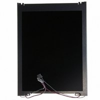
Page 15
... MECHANICAL SPECIFICATIONS (1) Front Side T-51639D084JU-FW-A-AB (AB) No. 2005-0392 OPTREX CORPORATION Unit:mm Page 15/36 ...
Page 16
... Rear Side [Note] We recommend you referring to the detailed drawing for your design. Please contact our company sales representative when you need the detailed drawing. T-51639D084JU-FW-A-AB (AB) No. 2005-0392 OPTREX CORPORATION Unit:mm Page 16/36 ...
Page 17
... Contrast Ratio, Luminance, Response Time, Viewing Angle, Color Coordinates: Display Center Luminance Uniformity: point 1 ∼ 5 shown in a figure below *2) Definition of Contrast Ratio CR=ON (White) Luminance / OFF(Black) Luminance *3) Definition of Luminance Lw= ON (White) Luminance T-51639D084JU-FW-A-AB (AB) No. 2005-0392 Ta = 25°C, VCC = 3.3 V, Input Signals: Typ. Values shown in Section 6 MIN. CR θ = φ = 0° 300 Lw θ ...
Page 18
... Definition of Viewing Angle( θ , φ ) *7) Image Sticking Continuously display the test pattern shown in the figure below for two-hours. Then display a completely white screen. The previous image shall not persist more than two seconds at 25°C. Rows 382-386 T-51639D084JU-FW-A-AB (AB) No. 2005-0392 90% 10% Black tr ...
Page 19
... The judgment of the above tests should be made as follow: Pass: Normal display image, no damage of the display function. (ex. no line defect) Partial transformation of the module parts should be ignored. Fail: No display image, damage of the display function. (ex. line defect) T-51639D084JU-FW-A-AB (AB) No. 2005-0392 40°C, 90% RH, 240 h BETWEEN − 20°C (1h) and 80°C(1h), CONDITIONS ...